Flip chip nitride semiconductor light emitting diode

a technology of semiconductor light emitting diodes and flip chips, which is applied in the direction of bends, branching pipes, mechanical equipment, etc., can solve the problems of reducing the reliability of leds, reducing the luminous efficiency, and degrading luminance properties, so as to improve the p-electrode structure, reduce current crowding, and improve the effect of forward voltag

Active Publication Date: 2005-07-21
SAMSUNG ELECTRONICS CO LTD
View PDF7 Cites 61 Cited by
  • Summary
  • Abstract
  • Description
  • Claims
  • Application Information

AI Technical Summary

Benefits of technology

[0011] The present invention has been made to solve the foregoing problems of the prior art and it is therefore an object of the present invention to provide a nitride s...

Problems solved by technology

Such current crowding increases forward voltage while lowering the luminous efficiency of an active layer portion relatively remote from the n-electrode to...

Method used


Image

  • Flip chip nitride semiconductor light emitting diode
  • Flip chip nitride semiconductor light emitting diode
  • Flip chip nitride semiconductor light emitting diode

Examples


##ventive example 1

Inventive Example 1

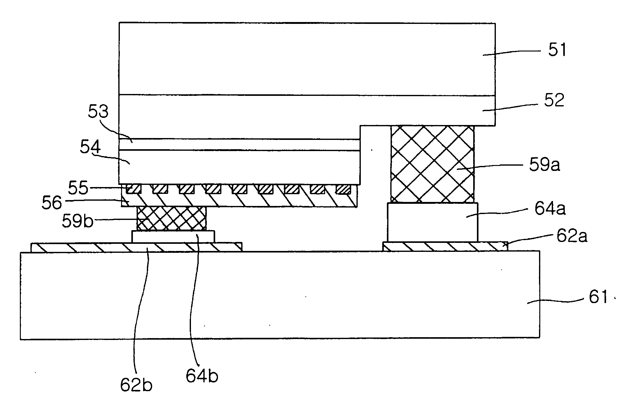
[0075] First, after loading a sapphire substrate into a MOCVD chamber, a GaN low temperature nucleation layer was grown as a buffer layer. Then, an n-doped semiconductor layer of an n-doped GaN film and an n-doped AlGaN layer, an active layer having a multiple quantum well structure of InGaN / GaN films and a p-doped nitride semiconductor layer of a p-doped GaN film were formed on the buffer layer to obtain a blue LED.

[0076] Next, a high reflectivity Ohmic contact layer of a mesh structure having an open area ratio of about 30% was formed on the p-doped nitride semiconductor layer, and then a resultant structure was heat treated at a temperature of about 500° C. The high reflectivity Ohmic contact layer of the Inventive Example 1 was made from Ni / Ag. Herein the open area ratio means the ratio of open areas with respect to the entire area (i.e., the area surround by the outermost periphery) as generally used in the specification.

[0077] Then, a metal barrier layer o...

##ventive example 2

Inventive Example 2

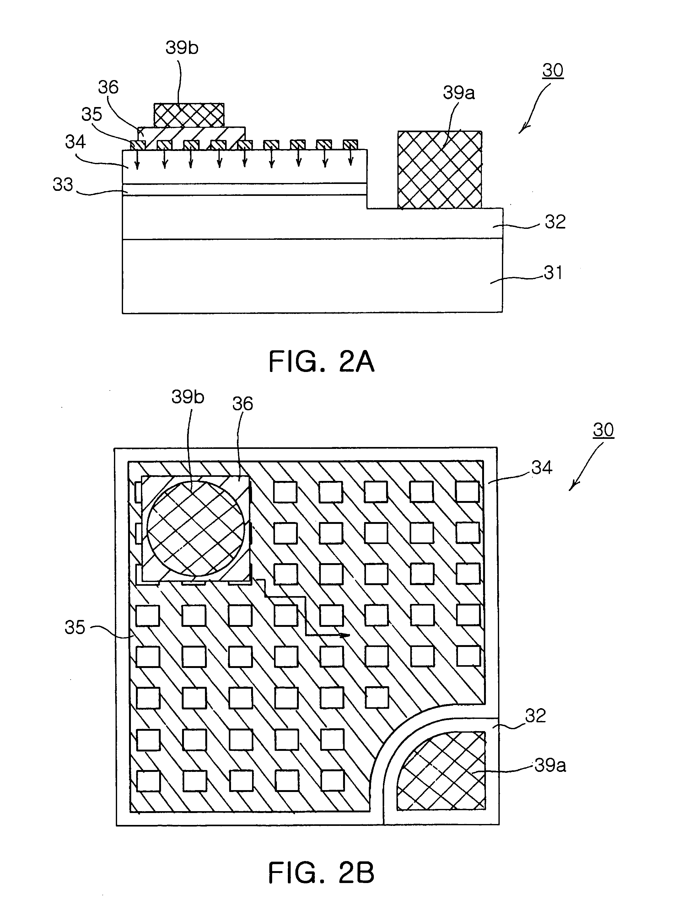
[0079] In the Inventive Example 2, a flip chip nitride semiconductor LED was prepared according to the same conditions as in the Inventive Example 1 except that a high reflectivity Ohmic contact layer of a mesh structure was patterned to have an open area ratio of about 50%. The flip chip nitride semiconductor LED prepared like this was coupled with a supporting substrate provided with a lead pattern as shown in FIG. 3B to produce a flip chip light emitting device.

##ventive example 3

Inventive Example 3

[0080] In the Inventive Example 3, a flip chip nitride semiconductor LED was prepared according to the same conditions as in the Inventive Example 1 except that a high reflectivity Ohmic contact layer of a mesh structure was patterned to have an open area ratio of about 70%. The flip chip nitride semiconductor LED prepared like this was coupled with a supporting substrate provided with a lead pattern as shown in FIG. 3B to produce a flip chip light emitting device.


PUM


Abstract

The invention relates to a nitride semiconductor LED, wherein an n-doped nitride semiconductor layer is formed on a transparent substrate. An active layer is formed on the n-doped nitride semiconductor layer. A p-doped nitride semiconductor layer is formed on the active layer. A high reflectivity Ohmic contact layer of a mesh structure is formed on the p-doped nitride semiconductor layer and has a number of open areas for exposing the p-doped nitride semiconductor layer. A metal barrier layer is formed on at least a top region of the high reflectivity Ohmic contact layer. A p-bonding electrode is formed on the metal barrier layer. An n-electrode is formed on the n-doped nitride semiconductor layer.

Description

CLAIM OF PRIORITY [0001] This application claims the benefit of Korean Patent Application No. 2004-3960 filed on Jan. 19, 2004, in the Korean Intellectual Property Office, the disclosure of which is incorporated herein by reference. BACKGROUND OF THE INVENTION [0002] 1. Field of the Invention [0003] The present invention relates to a nitride semiconductor Light Emitting Diode (LED), and more particularly, to a flip chip nitride semiconductor LED of excellent electric characteristics and luminance. [0004] 2. Description of the Related Art [0005] Recently, a nitride semiconductor LED as an optical device for generating blue or green wavelength light is made from semiconductor material expressed by an equation of AlxInyGa(1−x−y)N (wherein 0≦x≦1, 0≦y≦1 and 0≦x+y≦1). Considering lattice match, nitride semiconductor crystals are grown on a substrate such as a sapphire substrate that is used for the growth of nitride single crystals. Since the sapphire substrate is electrically insulated, ...

Claims


Application Information

Patent Timeline
IPC IPC(8): H01L33/10H01L33/06H01L33/32H01L33/38H01L33/46H01L33/62
CPCH01L33/32H01L33/387Y10S257/918H01L33/44H01L33/405H01L2224/14H01L2224/16225F16L19/0218F16L43/00F16L41/021
Inventor KIM, HYUN KYUNGJEONG, YOUNG JUNEKIM, YONG CHUN
Owner SAMSUNG ELECTRONICS CO LTD
Why Eureka
Try Eureka