Examination apparatus for biological sample and chemical sample

a biological sample and chemical sample technology, applied in the field of sensors and systems, can solve the problems of degrading the electric insulation between devices and the characteristics of devices, and achieve the effect of low cost and easy measurement of biological and chemical materials

Inactive Publication Date: 2005-07-21
HITACHI LTD
View PDF23 Cites 207 Cited by
  • Summary
  • Abstract
  • Description
  • Claims
  • Application Information

AI Technical Summary

Benefits of technology

[0006] Starting with the gene test and the protein test, the system capable of easily measuring biological and chemical materials has been demanded in various fields. In order to meet such demands, the inventors of the present invention examine the wireless sensor chip (hereinafter, referred to as sensor chip) in which a sensor for measuring a biological material such as DNA, a chemical material, ion, and physical quantity

Problems solved by technology

Also, the problem that the device characteristics and the electric insulation between devices are degraded due to the penetration of positive ions into the device forming region in a

Method used


Image

  • Examination apparatus for biological sample and chemical sample
  • Examination apparatus for biological sample and chemical sample
  • Examination apparatus for biological sample and chemical sample

Examples


Embodiment Construction

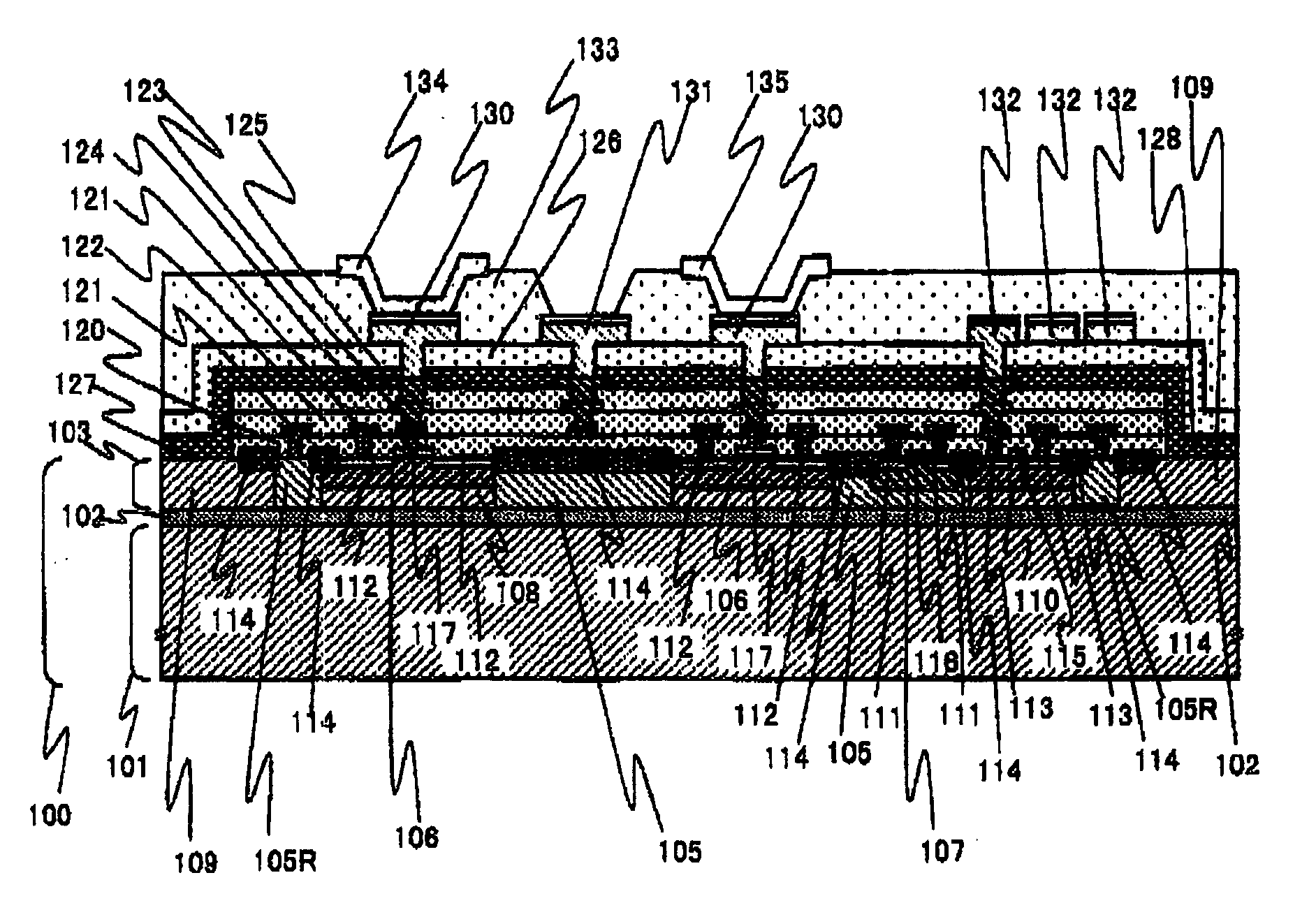
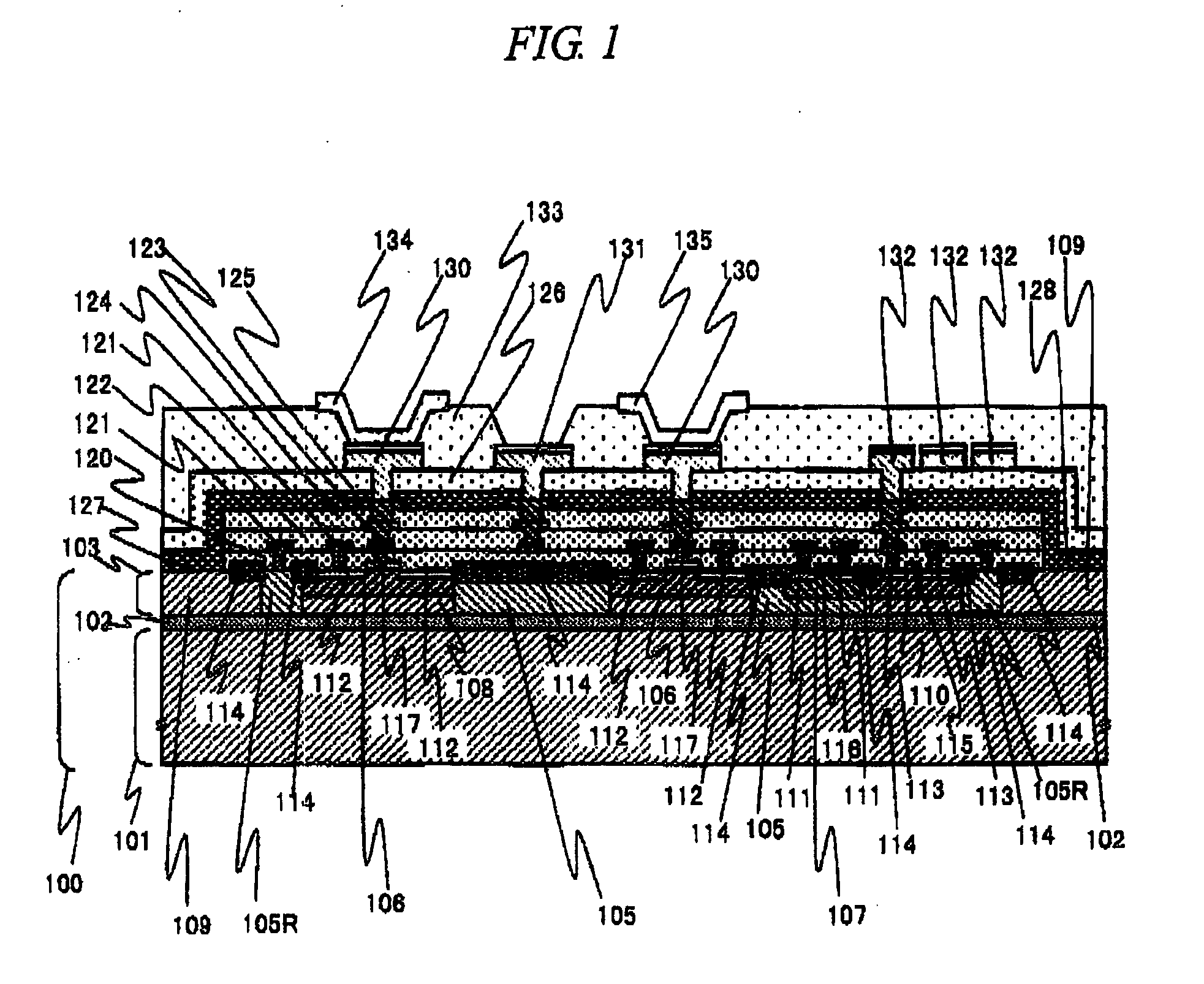
[0031] Hereinafter, embodiments of the present invention will be described in detail with reference to the accompanying drawings. Note that components having the same function are denoted by the same reference symbols throughout the drawings for describing the embodiments, and the repetitive description thereof will be omitted.

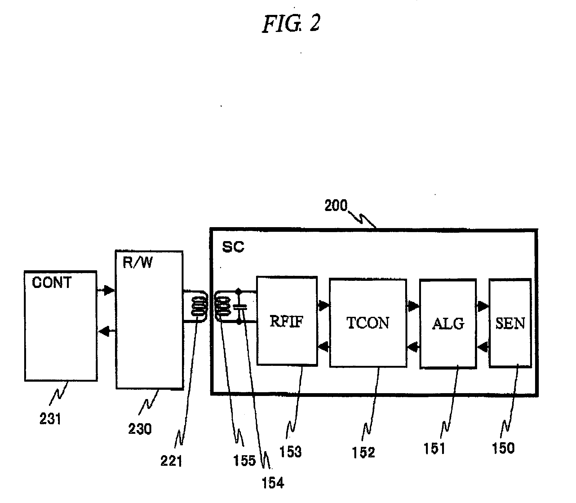
[0032]FIG. 2 shows an example of the measurement system using the sensor chip. First, a sensor chip 200 will be described. A sensor block 150 is comprised of a sensor such as an ISFET, a thermometer, and a photodiode. It is also possible to use a plurality of sensors or several types of sensors to form the sensor block 150. A sensor analog block 151 includes a signal processing circuit such as an amplifier for amplifying sensing signals from the sensor block 150 and an A / D converter for converting amplified sensing signals to digital signals and a sensor control circuit for controlling the sensor block 150. A communication control circuit block 152 controls t...


PUM


Abstract

A wireless sensor chip suitable for the compact, high-sensitive, and low-cost examination apparatus for easily examining a biological material such as gene at low cost is provided. A sensor chip is formed on an SOI substrate, and an n type semiconductor layer on which a pMOS transistor is formed and a p type semiconductor layer on which an nMOS transistor is formed are isolated by a pn junction. Therefore, the p type semiconductor layer at the outermost portion (chip edge portion to be in contact with solution) is set to floating, and the maximum potential and the minimum potential of the chip are supplied to an n type semiconductor layer and a p type semiconductor layer inside the outermost portion, respectively. Also, the chip is covered with an ion impermeable insulating film for reducing the penetration of positive ions through the oxide layer.

Description

CROSS-REFERENCE TO RELATED APPLICATION [0001] The present application claims priority from Japanese Patent Application JP 2004-012596 filed on Jan. 21, 2004, the content of which is hereby incorporated by reference into this application. TECHNICAL FIELD OF THE INVENTION [0002] The present invention relates to a sensor and a system, in which the sensor is put into or comes into contact with a sample and results thereof are transmitted wirelessly to an external device. As the examples of the system mentioned above, a system for detecting biological materials such as nucleic acid, protein, antigen, and antibody and a system for measuring physical and chemical quantity such as temperature, pressure, light, and ion concentration can be shown. BACKGROUND OF THE INVENTION [0003] Japanese Patent Laid-Open Application No. 2002-14072 discloses an integrated circuit device called an integrated sensor device, in which a sensor portion, a control unit for processing the signals representing the ...

Claims


Application Information

Patent Timeline
IPC IPC(8): H01L21/768G01N27/414H01L21/822H01L21/8238H01L23/522H01L27/04H01L27/08H01L27/092H01L27/12H01L29/786
CPCG01N27/414H01L51/0098G01N27/4148H01L27/1203H10K30/671
Inventor YAZAWA, YOSHIAKIWATANABE, KAZUKIKAMAHORI, MASAOKUNIMOTO, YUKINORI
Owner HITACHI LTD
Why Eureka
Try Eureka