Thin film transistors and semiconductor constructions

a technology of thin film transistors and semiconductor constructions, applied in the direction of transistors, semiconductor devices, electrical equipment, etc., can solve the problems of high concentration of broken or “dangling” si bonds, loss of data, and rise to potential barriers at grain boundaries

Inactive Publication Date: 2005-07-21
MICRON TECH INC
View PDF64 Cites 9 Cited by
  • Summary
  • Abstract
  • Description
  • Claims
  • Application Information

AI Technical Summary

Problems solved by technology

Without refreshing, the output of a dynamic memory cell will drift towards intermediate or indeterminate voltages, effectively resulting in loss of data.
The crystalline structure breaks down at the grain boundaries, giving rise to a high concentration of broken or “dangling” Si bonds.
These dangling bonds “trap” carriers and give rise to potential barriers at the grain boundaries.
These potential barriers impede the flow of carriers in polysilicon, thus reducing conductivity compared to bulk silicon.
Greater current leakage means that more power is required to replace the leaking current to maintain an SRAM cell transistor in its desired powered-on state.
Such leakage is particularly adverse in laptop computers, where desired power consumption when a cell's state is not being changed would be desired to be very low to extend battery life.
Current state-of-the-art TFTs provide low standby current at the expense of ON current, or at the expense of additional process complexity.
However, the existing ion implantation techniques of providing fluorine into a polycrystalline thin film is not without drawbacks.
For example, the implantation undesirably damages the thin film layer and typically creates more dangling bonds inherent from the implantation process.
Further, a large percentage of the fluorine does not reach the grain boundaries, even upon diffusion, and is therefore ineffective for the purpose of passivation, as ion implantation distributes the fluorine uniformly throughout the grains and grain boundaries.

Method used


Image

  • Thin film transistors and semiconductor constructions
  • Thin film transistors and semiconductor constructions
  • Thin film transistors and semiconductor constructions

Examples


Embodiment Construction

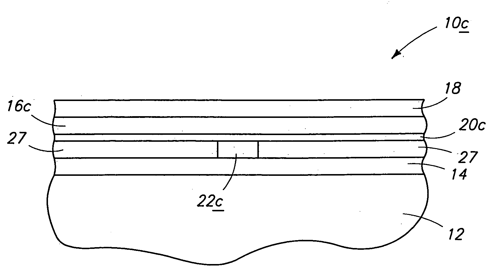
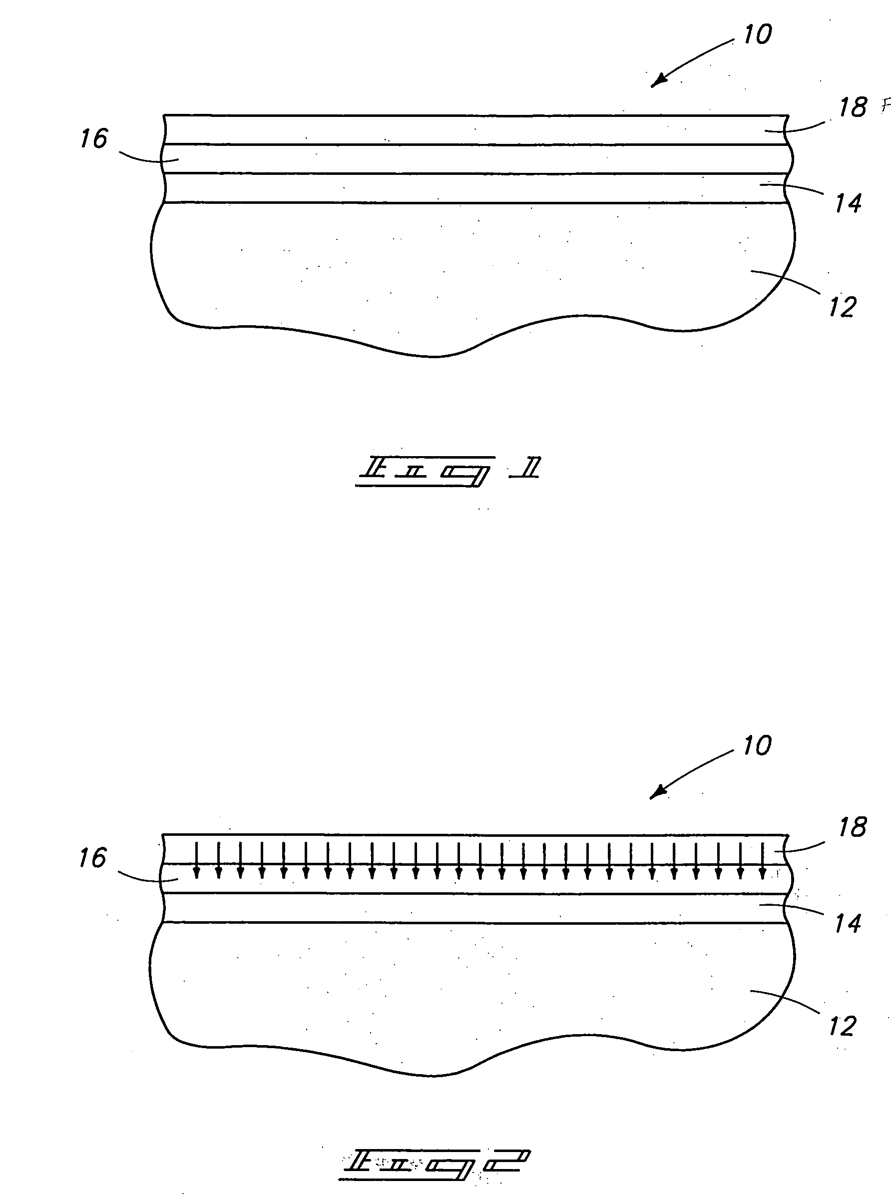
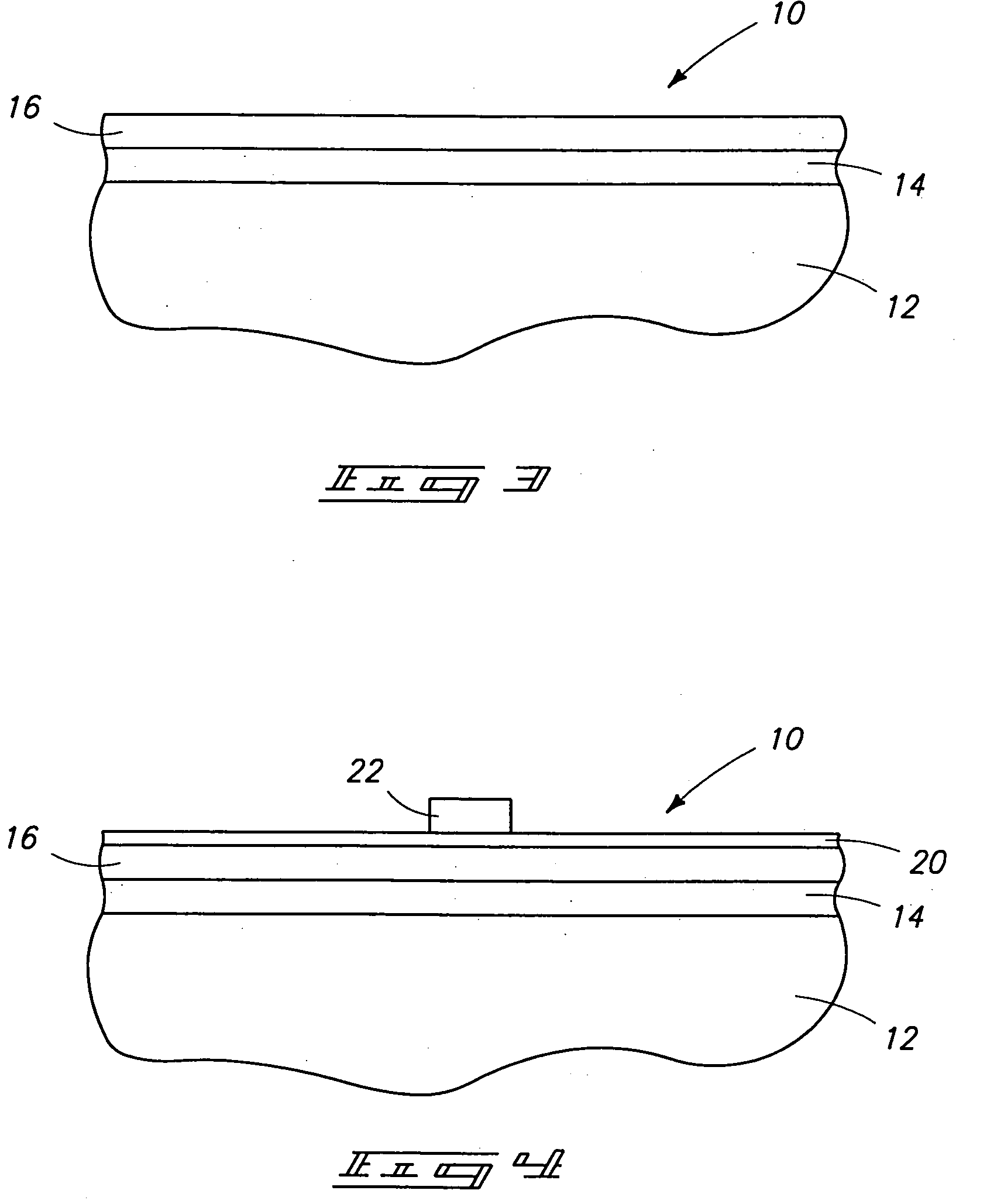
[0023] This disclosure of the invention is submitted in furtherance of the constitutional purposes of the U.S. Patent Laws “to promote the progress of science and useful arts” (Article 1, Section 8).

[0024] In accordance with one aspect of the invention, a method of forming a thin film transistor relative to a substrate comprises the following steps: [0025] providing a thin film transistor layer of polycrystalline material on a substrate, the polycrystalline material comprising grain boundaries; [0026] providing a fluorine containing layer adjacent the polycrystalline thin film layer; [0027] annealing the fluorine containing layer at a temperature and for a time period which in combination are effective to drive fluorine from the fluorine containing layer into the polycrystalline thin film layer and incorporate fluorine within the grain boundaries to passivate said grain boundaries; and [0028] providing a transistor gate operatively adjacent the thin film transistor layer.

[0029] In...


PUM

PropertyMeasurementUnit
pressureaaaaaaaaaa
temperaturesaaaaaaaaaa

Abstract

A method of forming a thin film transistor relative to a substrate includes, a) providing a thin film transistor layer of polycrystalline material on a substrate, the polycrystalline material comprising grain boundaries; b) providing a fluorine containing layer adjacent the polycrystalline thin film layer; c) annealing the fluorine containing layer at a temperature and for a time period which in combination are effective to drive fluorine from the fluorine containing layer into the polycrystalline thin film layer and incorporate fluorine within the grain boundaries to passivate said grain boundaries; and d) providing a transistor gate operatively adjacent the thin film transistor layer. The thin film transistor can be fabricated to be bottom gated or top gated. A buffering layer can be provided intermediate the thin film transistor layer and the fluorine containing layer, with the buffering layer being transmissive of fluorine from the fluorine containing layer during the annealing. Preferably, the annealing temperature is both sufficiently high to drive fluorine from the fluorine containing layer into the polycrystalline thin film layer and incorporate fluorine within the grain boundaries to passivate said grain boundaries, but sufficiently low to prevent chemical reaction of the fluorine containing layer with the polycrystalline thin film layer.

Description

TECHNICAL FIELD [0001] This invention relates to thin film transistors and to methods of forming thin film transistors. BACKGROUND OF THE INVENTION [0002] As circuit density continues to increase, there is a corresponding drive to produce smaller and smaller field effect transistors. Field effect transistors have typically been formed by providing active areas within a bulk substrate material or within a complementary conductivity type well formed within a bulk substrate. Although the field effect transistor feature size is reducing with advances in process technology, even greater packing density can be achieved by forming transistors in thin films deposited over insulating layers, such as oxide. These transistors are commonly referred to as “thin film transistors” (TFTs). [0003] With TFTs, a thin film of semiconductive material is first provided. A central channel region of the thin film is masked, while opposing adjacent source / drain regions are doped with an appropriate p or a t...

Claims


Application Information

Patent Timeline
Patent Type & Authority Applications(United States)
IPC IPC(8): H01L21/336H01L21/77H01L21/84H01L29/04H01L29/786
CPCH01L27/1214H01L29/04H01L29/6675H01L29/78678H01L29/66765H01L29/78672H01L29/78675H01L29/66757H01L27/127
Inventor SANDHU, GURTEJ S.BATRA, SHUBNEESHFAZAN, PIERRE C.
Owner MICRON TECH INC
Why Eureka
Try Eureka