Wiring substrate

Inactive Publication Date: 2005-07-21
RICOH PRINTING SYST
View PDF10 Cites 10 Cited by
  • Summary
  • Abstract
  • Description
  • Claims
  • Application Information

AI Technical Summary

Benefits of technology

[0013] It is therefore an object of the invention to provide a wiring substrate and a method of manufacturing the same whereby the undesired spreading of metal microparticles and disconnection during the formation of a metal wire using metal microparticles can be prevented and a superior mass productivity can be obtained.
[0014] As a result of analysis of the surface states of various substrates in an attempt to achieve the aforementioned object of the invention, it has been found that by using a substrate provided with appropriate surface pits and projections and with an appropriate level of liquid repellency, the spreading of metal wires to a greater degree than is desired and disconnection can be prevented.
[0015] As a first means of achieving the aforementioned object, the invention provides a wiring substrate comprising a substrate, an organic membrane formed on the substrate, and a metal wire formed on the organic membrane, wherein a mean deviation Ra of the profi

Problems solved by technology

When drawing a wire on a substrate by coating it with a dispersion liquid of metal microparticles, if the liquid repellency of the substrate is not sufficient, the dispersion liquid of metal microparticles could spread further than is necessary, thereby failing to draw a wire of desired width.
Conversely, if the liquid repellency is too high, the droplet of the dispersion liquid that has been dropped on the substrate could be repelled, possibly resulting in a disconnection, particularly when the intended wire is a long one.
However, although a desired wire can be drawn according to this method i

Method used


Image

  • Wiring substrate
  • Wiring substrate
  • Wiring substrate

Examples


example 1

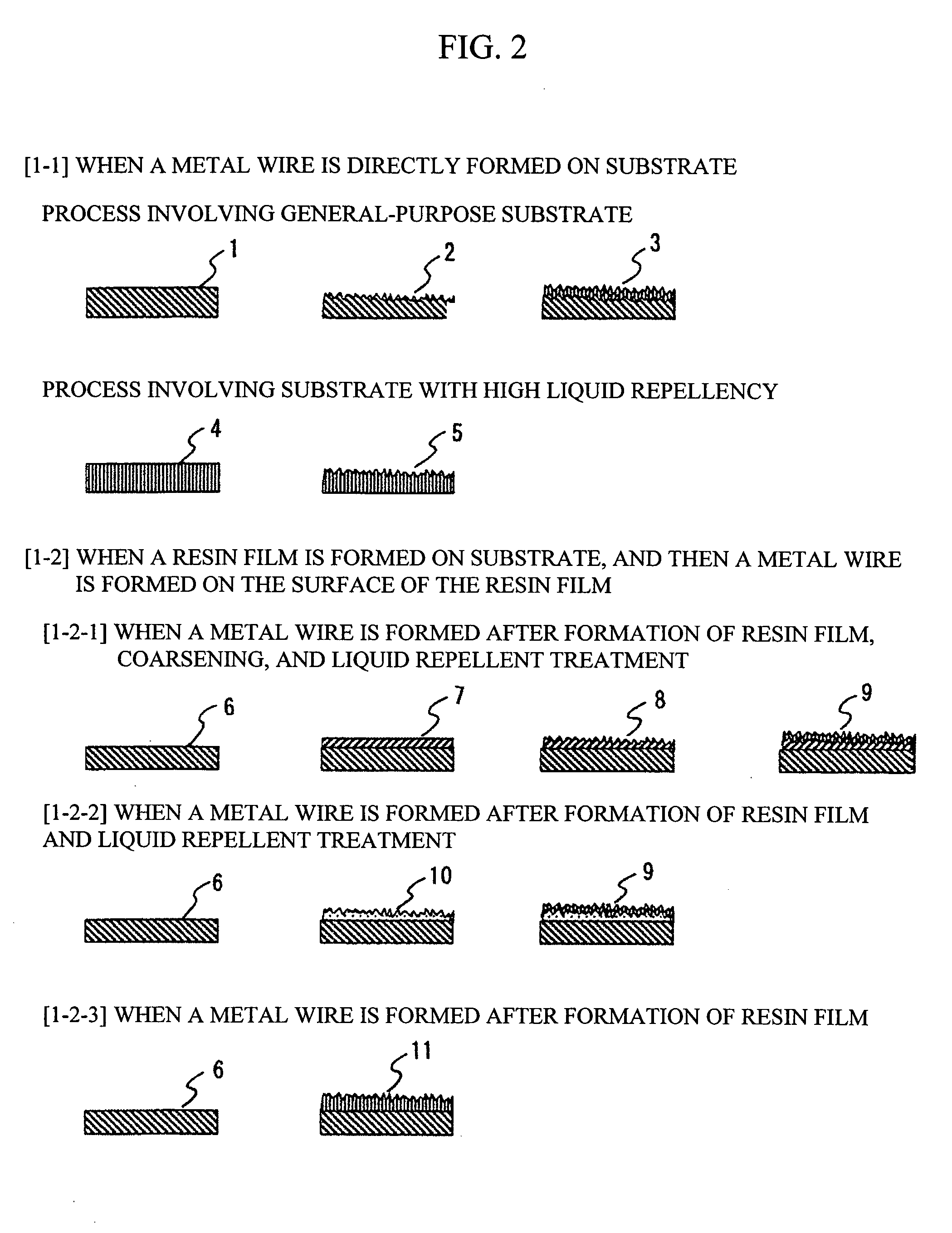
[0122] This example relates to the method of preparing a substrate using a general-purpose substrate (see FIG. 2(1-1)).

1. Preparation of a Substrate for Wiring

[0123] The surface of a glass substrate measuring 100×50 mm and having a thickness of 1 mm was coarsened using a sandblasting apparatus (Pneuma-Blaster SFK 2 from Fuji Manufacturing Co., Ltd.). The polishing material used was a Fuji Random A ceramic polishing material from Fuji Manufacturing Co., Ltd. (where a particle range of 53 to 75 μm was used for Ra<1 μm and a range of 180 to 212 μm was used for Ra≧1 μm). A surface with varying Ra was formed by varying the blast time.

[0124] To impart liquid repellency to the substrate, the thus coarsened glass substrate was then dipped in a 0.5% by weight solution of Compound 17 (with a Frorinart PF-5080 solvent from 3M Company). The substrate was then raised and heated at 130° C. for 15 minutes to obtain a substrate for wiring.

[0125] Table 1 shows the Ra values of the substrate and...

example 2

[0139] After the coarsening of the surface, substrates for wiring were prepared by the same procedure as in Example 1 except that a 0.5% by weight solution of Compounds 18 to 28 (with Frorinart PF-5080 solvent from 3M Company) was used instead of the 0.5% by weight solution of Compound 17 (with Frorinart PF-5080 solvent from 3M Company).

[0140] The substrates were provided with wiring by the same method as in Example 1. In the present example, since the objective was to examine the difference in the condition of the wires formed due to different liquid repellent agents, the width of wires was limited to 60 μm. The results of the examination are shown in Table 4.

TABLE 4Condition of wires formed on substrates with different deviation of profile when different liquid repellent agents were usedRaLiquid repellent agent used (Compound)(μm)1718192021222324252627280.011C(112)C(112)C(115)C(115)S(88)S(88)S(92)S(92)C(111)C(113)C(111)C(113)0.036C(126)C(126)C(128)C(128)S(92)S(92)S(96)S(96)C(12...

example 3

[0143] The present example relates to the method of preparing a substrate using a highly liquid-repellent substrate (see FIG. 2 [1-1]).

1. Preparation of a Substrate for Wiring

[0144] The surface of a substrate made of polytetrafluoroethylene-ethylene copolymer and measuring 100×50 mm and having a thickness of 1 mm was coarsened using a sandblasting apparatus (an integral sandblasting apparatus SFK-2 from Fuji Manufacturing Co., Ltd.). The polishing material used was of ceramic type (zirconia beads from Fuji Manufacturing Co., Ltd., with a particle size ranging from 75 to 106 μm). Surfaces with various Ra were formed by varying the time of blast, thereby producing the substrates for wiring.

[0145] Table 5 shows the Ra and contact angle of the substrate thus prepared.

TABLE 5Condition of wires formed on substrates with different deviation of profileContact angleWidth ofwithwire drawn (μm)Ra (μm)water (°)1001500.041123CC0.057133CC0.063134XX0.078141XX0.57>150XX0.62>150XX1.17>150XX3.1...


PUM

PropertyMeasurementUnit
Widthaaaaaaaaaa
Nanoscale particle sizeaaaaaaaaaa
Contact angleaaaaaaaaaa

Abstract

A substrate is provided on which wires can be formed satisfactorily using a dispersion liquid of metal microparticles without causing disconnection or short circuit. The wiring substrate comprises a substrate, an organic membrane formed on the substrate, and a metal wire formed on the organic membrane. An arithmetic mean deviation Ra of the profile of the surface of the organic membrane where the metal wire is formed is not less than 60 nm and not more than 5×10⁻² D, where D is the width of the metal wire. The contact angle with respect to water on the surface of the organic membrane where the metal wire is formed is not less than 110°.

Description

BACKGROUND OF THE INVENTION [0001] 1. Field of the Invention [0002] The invention relates to a wiring substrate on which metal wires are formed. [0003] 2. Description of Related Art [0004] Wiring substrates are used in many products, including OA equipment such as personal computers, printers, scanners, and various types of memory; household appliances such as television sets, audio equipment, cleaners, refrigerators, microwave ovens, and rice cookers; and transportation means such as automobiles, trains, ships, and airplanes. Metal wires are formed on such wiring substrates, and LSIs, ICs, transistors, diodes, capacitors, and resistors, for example, are mounted in accordance with the metal wires. [0005] While the wiring substrates are in many cases formed by plating, methods have recently been disclosed whereby metal wires are formed by drawing or depicting them using a dispersion liquid of metal microparticles and then subjecting the drawn wires to heating or other processes. Exam...

Claims


Application Information

Patent Timeline
IPC IPC(8): H05K1/09B32B1/00B32B9/00C08J7/12C09K3/18H05K1/02H05K3/10H05K3/12H05K3/38
CPCH05K3/1208H05K3/125H05K3/386Y10T428/24917H05K2201/0209H05K2203/013H05K2203/1173H05K2201/015
Inventor SASAKI, HIROSHIKUROSAWA, MAKOTOSHIMIZU, KAZUO
Owner RICOH PRINTING SYST
Why Eureka
Try Eureka