Nickel salicide processes and methods of fabricating semiconductor devices using the same

a technology of nickel salicide and process, applied in the direction of semiconductor devices, basic electric elements, electrical apparatus, etc., can solve the problems of reducing the drivability of the short-channel mos transistor, narrowing the width increasing the electrical resistance of the gate electrode, so as to enhance the thermal stability of the mono-nickel mono-silicide layer

Inactive Publication Date: 2005-07-21
SAMSUNG ELECTRONICS CO LTD
View PDF13 Cites 37 Cited by
  • Summary
  • Abstract
  • Description
  • Claims
  • Application Information

AI Technical Summary

Benefits of technology

[0013] Embodiments of the invention provide a nickel salicide process capab

Problems solved by technology

Also, reduction of the channel length leads to a narrowing of the width of the gate electrode, which in turn increases the electrical resistance of the gate electrode.
In this case, however, the sheet resistances of the source/drain regions are increased, and the drivability of the short channel MOS transistor is degraded.
A method of forming a cobalt silicide layer is disclosed in U.S. Pat. No. 5,989,988 to linuma et al., entitled “Semiconductor Device

Method used


Image

  • Nickel salicide processes and methods of fabricating semiconductor devices using the same
  • Nickel salicide processes and methods of fabricating semiconductor devices using the same
  • Nickel salicide processes and methods of fabricating semiconductor devices using the same

Examples


Embodiment Construction

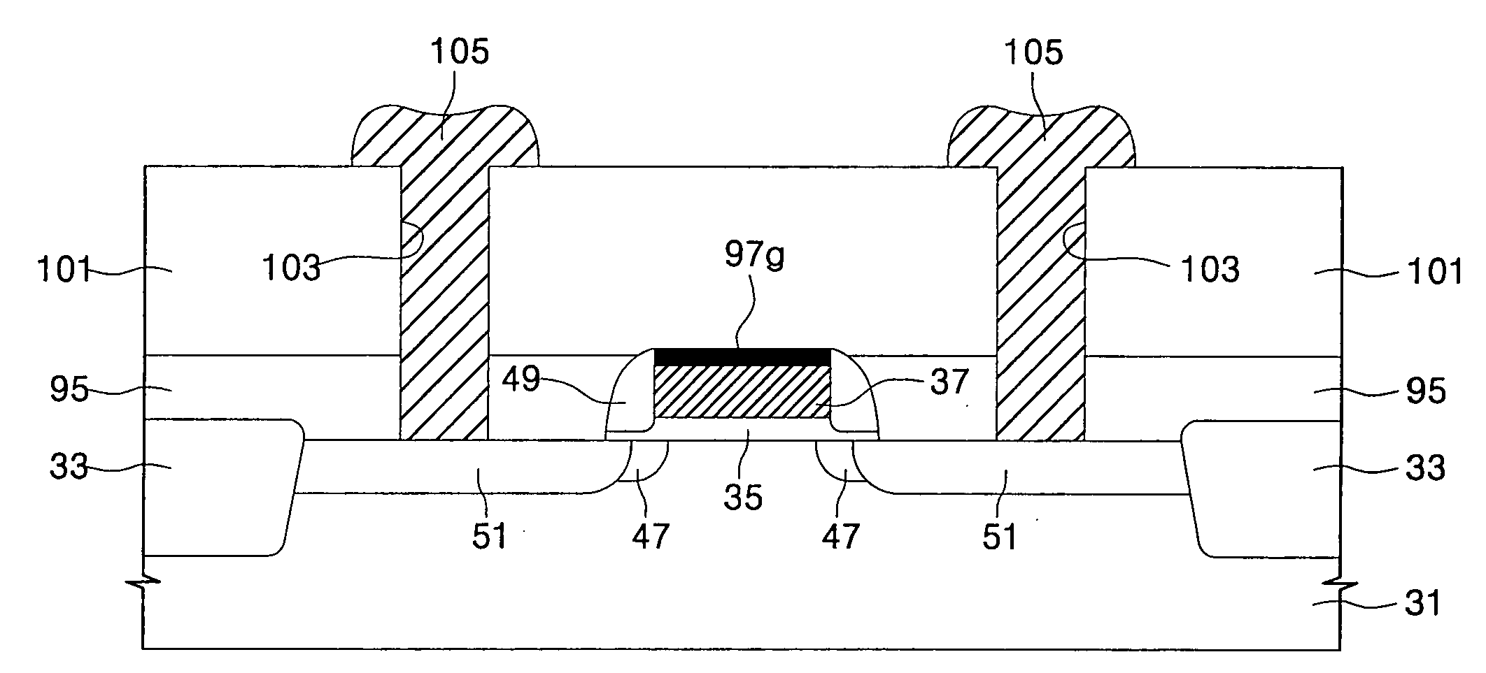
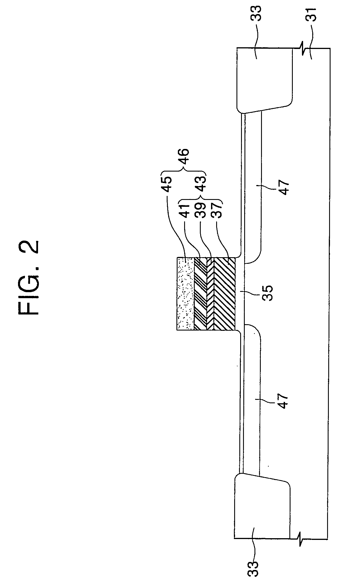
[0047] The present invention will now be described more fully hereinafter with reference to the accompanying drawings, in which preferred embodiments of the invention are shown. This invention may, however, be embodied in different forms and should not be construed as limited to the embodiments set forth herein. Rather, these embodiments are provided so that this disclosure will be thorough and complete, and will fully convey the invention to those skilled in the art. In the drawings, the thicknesses and relative dimensions of layers and regions may be exaggerated for clarity. Like numbers refer to like elements throughout the drawings and specification.

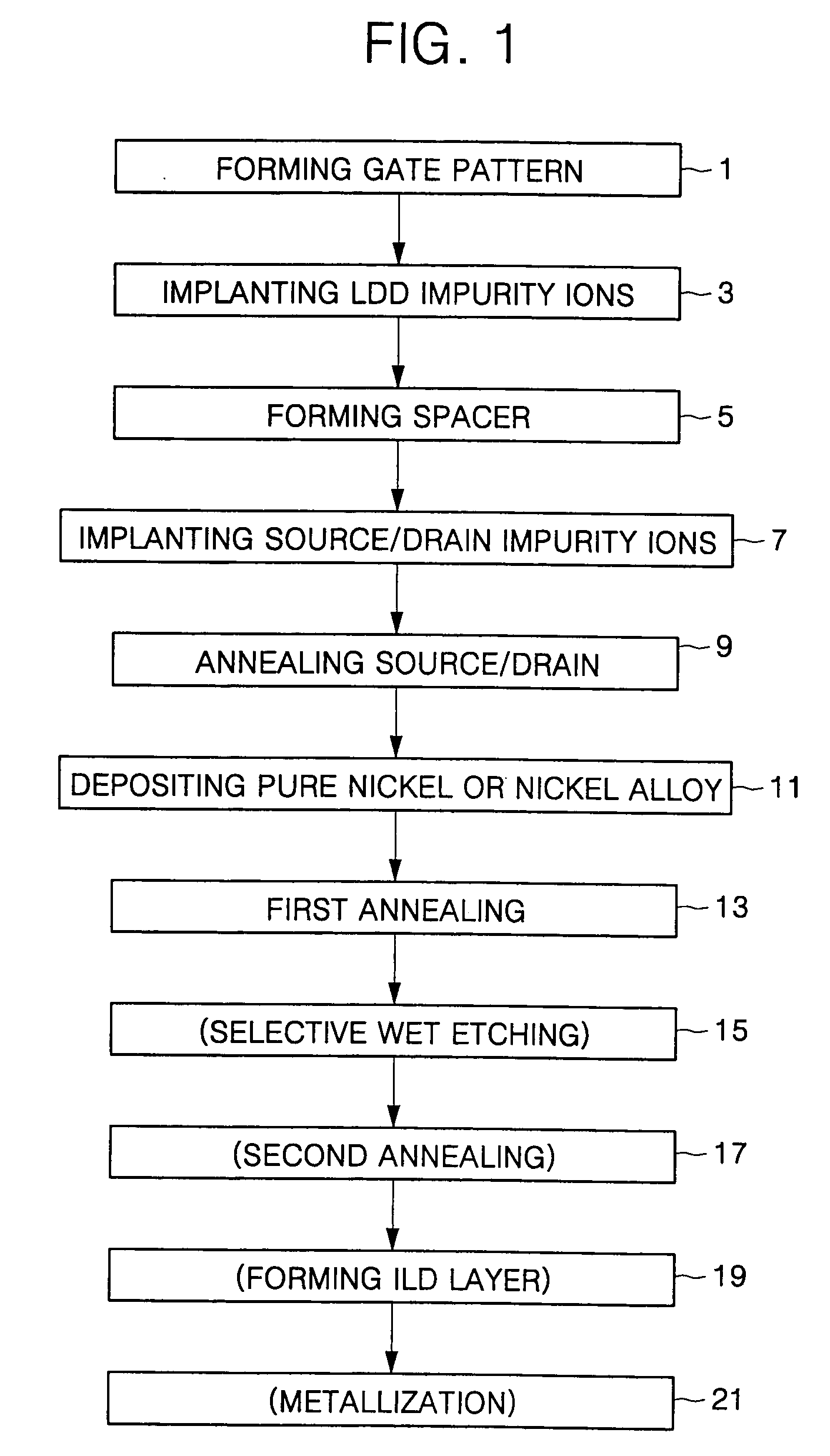
[0048]FIG. 1 is a process flow chart illustrating nickel salicide processes and methods of fabricating a semiconductor device using the same in accordance with embodiments of the present invention, and FIGS. 2 to 7 are cross-sectional views for explaining the nickel salicide processes and methods of fabricating a semiconductor devic...


PUM


Abstract

A nickel salicide process includes preparing a substrate having a silicon region and an insulating region containing silicon. Nickel is deposited on the substrate, and the nickel is annealed at a first temperature of 300° C. to 380° C. to selectively form a mono-nickel mono-silicide layer on the silicon region and to leave an unreacted nickel layer on the insulating region. The unreacted nickel layer is selectively removed to expose the insulating region and to leave the mono-nickel mono-silicide layer on the silicon region. Subsequently, the mono-nickel mono-silicide layer is annealed at a second temperature which is higher than the first temperature to form a thermally stable mono-nickel mono-silicide layer and without a phase transition of the mono-nickel mono-silicide layer.

Description

CROSS-REFERENCE TO RELATED APPLICATION [0001] A claim of priority is made to Korean Patent Application No. 2003-81255, filed Nov. 17, 2003, the contents of which are hereby incorporated herein by reference in their entirety. BACKGROUND OF THE INVENTION [0002] 1. Field of the Invention [0003] The present invention generally relates to methods of fabricating a semiconductor device and, more particularly, the present invention relates to nickel salicide processes and to methods of fabricating a semiconductor device using the same. [0004] 2. Description of the Related Art [0005] Discrete devices such as metal oxide semiconductor (MOS) transistors are widely employed in semiconductor devices. As the semiconductor devices become more highly integrated, it becomes necessary to reduce the scale of the MOS transistors. The resultant reduction in channel length of the MOS transistors can cause a short channel effect. Also, reduction of the channel length leads to a narrowing of the width of t...

Claims


Application Information

Patent Timeline
IPC IPC(8): H01L21/28H01L21/24H01L21/285H01L21/336H01L29/78
CPCH01L21/28052H01L29/665H01L21/28518H01L21/24
Inventor KIM, MIN-JOOKU, JA-HUMSUN, MIN-CHULROH, KWAN-JONG
Owner SAMSUNG ELECTRONICS CO LTD
Why Eureka
Try Eureka