
Semiconductor device and method of manufacturing the semiconductor device

Active Publication Date: 2005-07-28
SAMSUNG ELECTRONICS CO LTD
View PDF7 Cites 21 Cited by
  • Summary
  • Abstract
  • Description
  • Claims
  • Application Information

AI Technical Summary

Benefits of technology

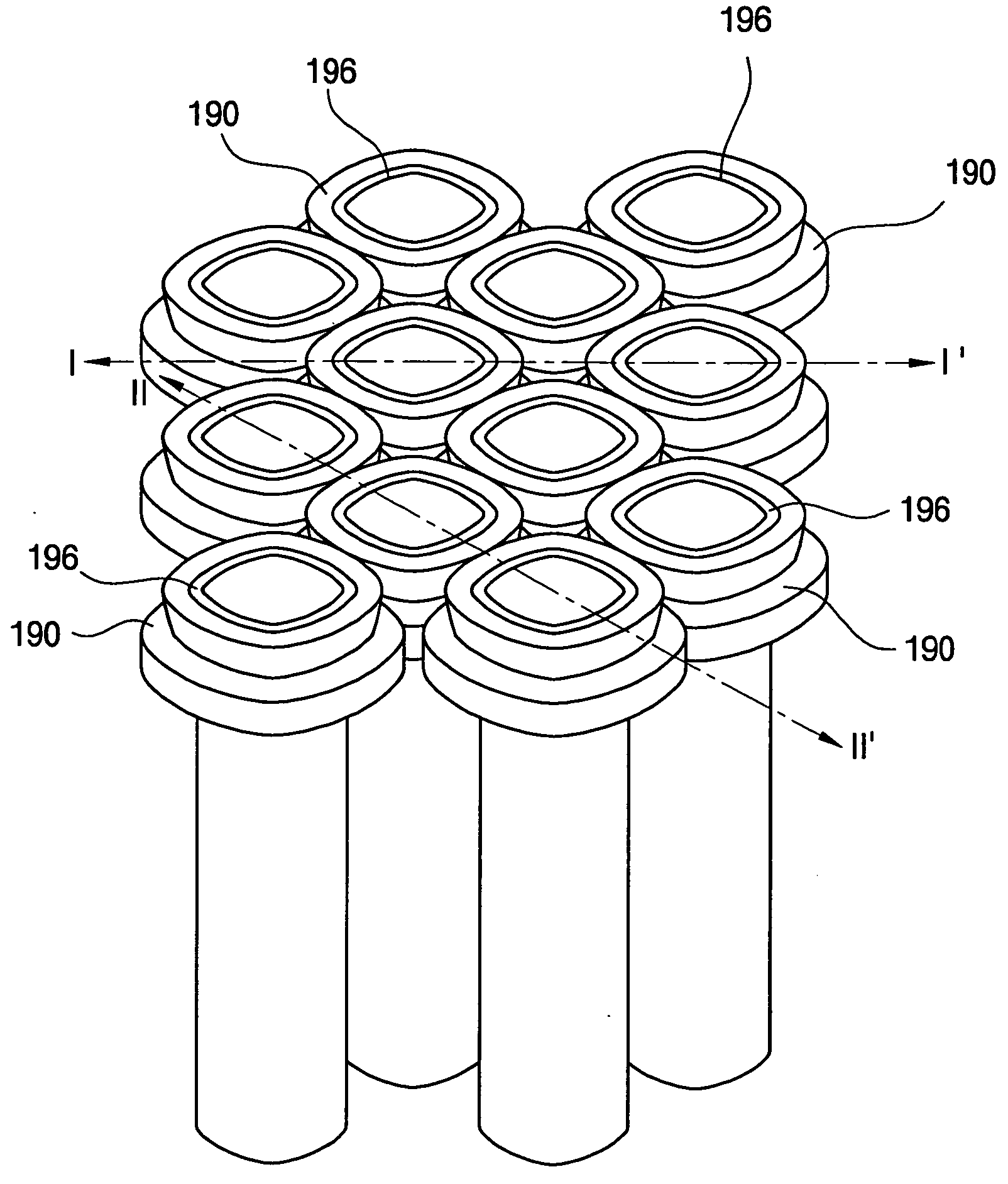
[0020] The present invention provides a semiconductor device with an improved structural stability in accordance with a simple stabilizing member and an extended effective area thereof.
[0021] The present invention also provides a method of manufacturing a semiconductor device having an improved structural stability.
[0022] In the present invention, since stabilizing members are provided to greatly improve structural stabilities of the capacitors, the capacitors may have very high height without collapse when the capacitors have extremely high aspect ratios. Therefore, the capacitors may have greatly enhanced capacitance in comparison with a conventional capacitor.

Problems solved by technology

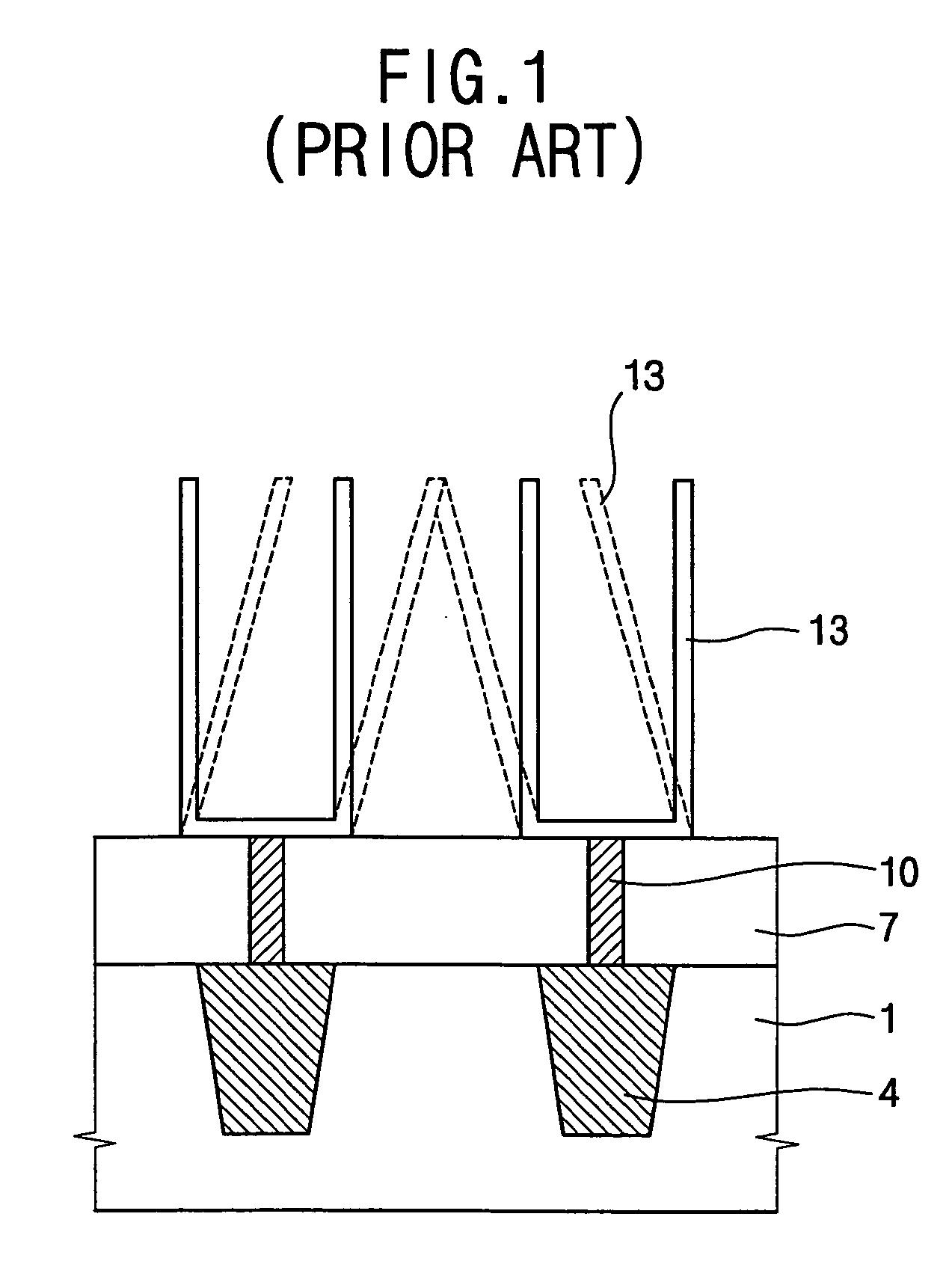
However, due to design constraints of the semiconductor memory device that include size decreases, the capacitor should have an increasingly large aspect ratio, defined as the ratio of the height to the width of the capacitor.
As a result, however, the capacitors having a high aspect ratio may mechanically collapse so that a so-called two-bit failure may occur between adjacent capacitors.
When the two-bit failure occurs in the semiconductor memory device, the semiconductor memory device may not properly operate.
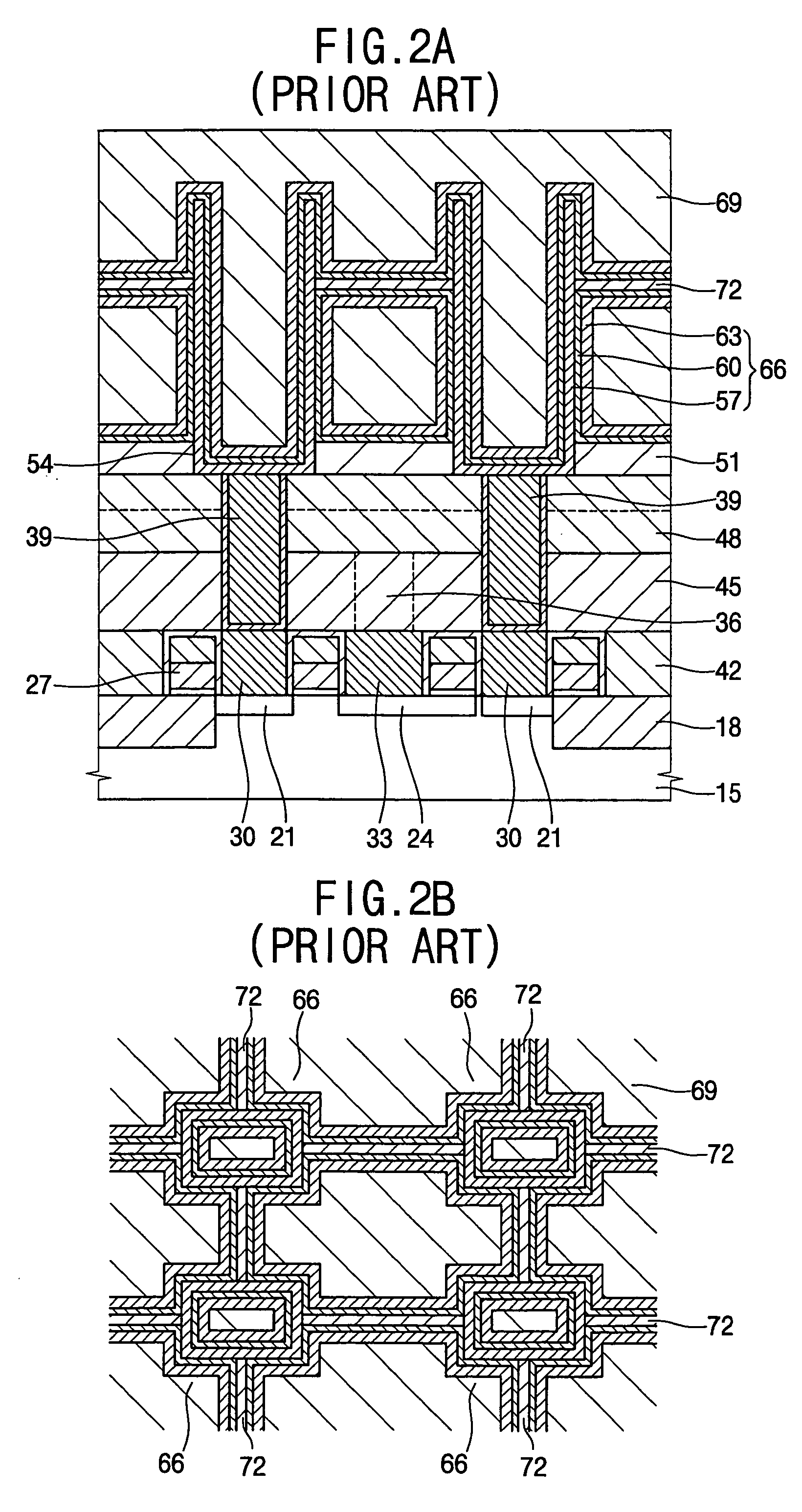
However, in the above-described semiconductor device, processes for manufacturing the semiconductor device are complicated because at least four beam-shaped insulating members 72 should be formed between the adjacent bottom electrodes 57 to improve the mechanical strength of the capacitor 66.
Thus, manufacturing cost and manufacturing time for the semiconductor device is increased.
As a result, the processes for manufacturing the semiconductor device including the capacitor 66 having the complex structure may have poor throughput.

Method used


Image

  • Semiconductor device and method of manufacturing the semiconductor device
  • Semiconductor device and method of manufacturing the semiconductor device
  • Semiconductor device and method of manufacturing the semiconductor device

Examples


Embodiment Construction

[0035] The present invention now will be described more fully hereinafter with reference to the accompanying drawings, in which embodiments of the invention are shown. In the drawings, the thickness of layers and regions are exaggerated for clarity. Like reference numerals refer to similar or identical elements throughout. It will be understood that when an element such as a layer, a region, or a substrate is referred to as being “on” or “onto” another element, it can be directly on the other element or intervening elements may also be present.

[0036]FIGS. 3A and 3B are cross-sectional views illustrating processing steps of forming underlying structures on a semiconductor substrate 100.

[0037] Referring to FIGS. 3A and 3B, the semiconductor substrate 100 is divided into an active region and a field region by forming an isolation layer 103 in the semiconductor substrate 100. The isolation layer 103 may be formed by an isolation process such as a shallow trench isolation (STI) process...


PUM

PropertyMeasurementUnit
Shapeaaaaaaaaaa
Electrical conductoraaaaaaaaaa
Selectivityaaaaaaaaaa

Abstract

A semiconductor device has a stabilizing member that encloses an upper portion of a storage electrode to improve structural stability. A dielectric layer and a plate electrode are successively formed on the storage electrode including a stabilizing member. Since the stabilizing member includes a protruding portion to support the storage electrode and an adjacent storage electrode, all of the storage electrodes in a unit cell of a semiconductor device are structured to prevent a collapse. Also, the semdevice can have a very high height without collapse when the capacitors have extremely high aspect ratios. Therefore, the capacitors may have greatly enhanced capacitance in comparison with a conventional capacitor.

Description

CROSS REFERENCE TO RELATED APPLICATION [0001] This application claims priority under 35 USC § 119 of Korean Patent Application No. 2004-4640, filed on Jan. 26, 2004, the contents of which are incorporated herein by reference in their entirety. BACKGROUND OF THE INVENTION [0002] 1. Field of the Invention [0003] The present invention relates to a semiconductor device and a method of manufacturing the semiconductor device. More particularly, the present invention relates to a capacitor having an improved structural stability and a method of manufacturing the capacitor. [0004] 2. Description of the Related Art [0005] In general, semiconductor memory devices such as dynamic random access memory (DRAM) devices or static random access memory (SRAM) devices can store data or information therein. The data or information is stored in the semiconductor memory devices, and also the data or information is read from the semiconductor memory devices. A typical single unit memory cell of the semico...

Claims


Application Information

Patent Timeline
IPC IPC(8): H01L21/02H01L21/8242H01L27/108
CPCH01L27/10817H01L28/91H01L27/10885H01L27/10852H10B12/318H10B12/033H10B12/482B29C45/38B29D11/00432B26D7/22
Inventor PARK, JE-MIN
Owner SAMSUNG ELECTRONICS CO LTD
Features
  • Generate Ideas
  • Intellectual Property
  • Life Sciences
  • Materials
  • Tech Scout
  • Unparalleled Data Quality
  • Higher Quality Content
  • 60% Fewer Hallucinations
Learn More