Check patentability & draft patents in minutes with Patsnap Eureka AI!

Radiation hardened MOS structure

a mos structure and hardening technology, applied in the field of integrated circuit technology, can solve the problems of affecting performance and system efficiency, affecting the performance and system efficiency of the device, and the drift of electrical parameters and/or logic failure,

Inactive Publication Date: 2005-07-28
STMICROELECTRONICS SRL
View PDF9 Cites 10 Cited by
  • Summary
  • Abstract
  • Description
  • Claims
  • Application Information

AI Technical Summary

Problems solved by technology

Semiconductor devices and integrated circuits (ICs) used in outer space, for example, in a satellite, are subjected to severe environmental conditions that may cause electrical parameter drift and / or logic failure.
The resulting charge carriers are often trapped in the various oxide layers of the devices.
As a result, leakage currents of the transistors, and consequently, of the IC device will affect performance and system efficiency.
However, the mentioned technique is not as effective when applied to LOCOS isolation regions.
Although the Vt of the incidental transistor of the LOCOS isolation regions may be adjusted so that the Vt shift due to charge trapped in the thick oxide is relatively small, the resulting isolation region will have an unacceptably low breakdown voltage.
However, this approach is limited by the doping concentration of the relatively thick oxide layer.
The holes that escape the initial recombination are relatively immobile and remain near their point of generation, thereby causing negative voltage shifts in the electrical characteristics of the MOS device.
But over a longer period of time, exceeding one second, the holes undergo a rather anomalous stochastic hopping transport through the oxide in response to any electric fields present.
This long-term radiation-induced voltage shift is a common form of radiation damage in MOS devices.
Radiation-induced generation and trapping of holes is a problem in both gate oxide and field or silicon oxide of MOS devices.
The properties of field oxides are not as well controlled as those of gate oxides.
This study that considers true ring MOS was conducted by CERN at Geneva, it works but is not good for design in terms of occupied area and true W / L calculation.

Method used


Image

  • Radiation hardened MOS structure
  • Radiation hardened MOS structure
  • Radiation hardened MOS structure

Examples


Embodiment Construction

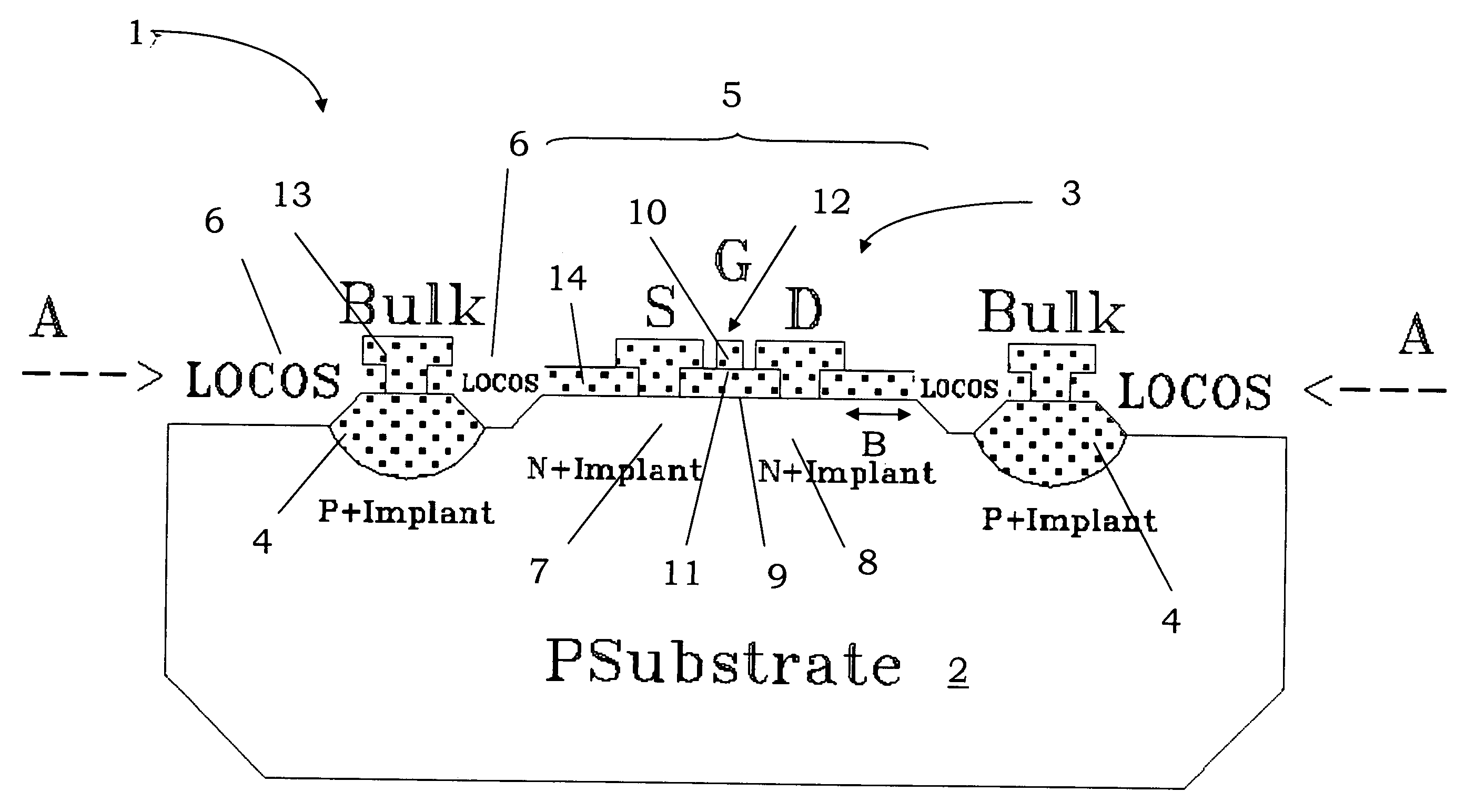
[0046] Embodiments of the invention relate particularly, but not exclusively, to a radiation hardened MOS structure integrated on a semiconductor substrate and the following description is made with reference to this field of application for convenience of illustration only.

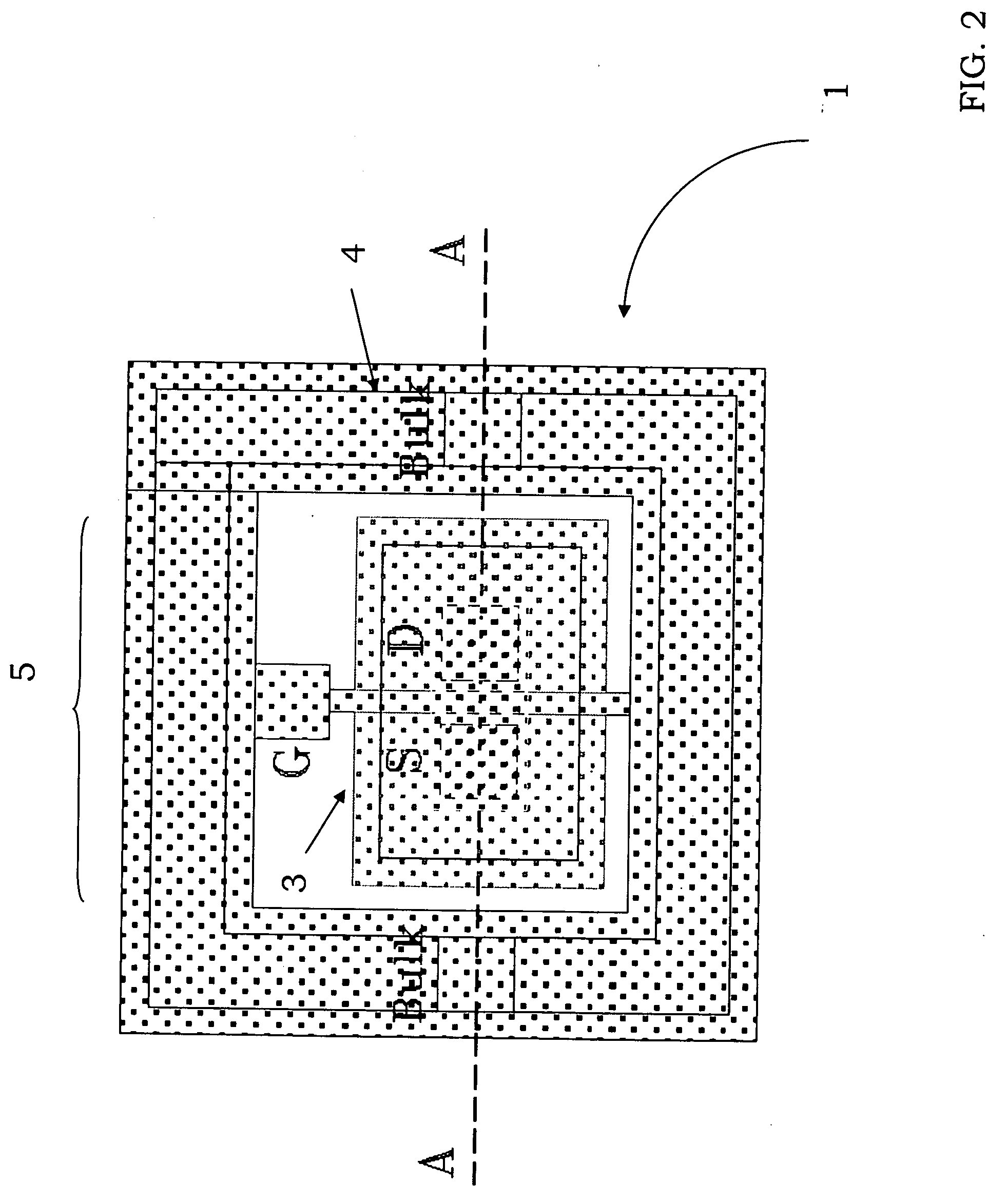
[0047] With reference to FIGS. 2 to 5, a radiation hardened MOS structure is described. In these FIGURES the cross-sections shown through a semiconductor wafer are not drawn to scale but rather to highlight major features of the invention.

[0048] According to an aspect of the invention, the radiation hardened MOS structure 1, integrated on a semiconductor substrate 2, comprises NMOS transistor 3 and a guard ring element 4 surrounding the NMOS transistor 3.

[0049] The NMOS transistor 3 is formed in active area 5 surrounded by a thick isolation layer 6, for example a thick oxide layer of LOCOS type.

[0050] The NMOS transistor 3 comprises a drain region 7 and a source region 8, formed by an N-type implant in the se...


PUM


Abstract

A radiation hardened MOS structure is integrated on a semiconductor substrate. The structure includes a MOS transistor realized in an active area surrounded by an isolation layer. The MOS transistor includes a channel region delimited by opposed source and drain regions of a first type of conductivity and a gate region formed above the channel and insulated from it by a thin oxide layer. The radiation hardened MOS structure includes a guard ring element of a second type of conductivity, formed in the semiconductor substrate under the isolation layer. The source and drain regions are spaced away from the isolation layer.

Description

PRIORITY CLAIM [0001] The present application claims priority from European Patent Application No. 03293117.2 filed Dec. 11, 2003, the disclosure of which is hereby incorporated by reference. BACKGROUND OF THE INVENTION [0002] 1. Technical Field of the Invention [0003] The present invention relates to an integrated circuit technology and, more particularly, to a radiation-hardened circuit technology. [0004] 2. Description of Related Art [0005] Semiconductor devices and integrated circuits (ICs) used in outer space, for example, in a satellite, are subjected to severe environmental conditions that may cause electrical parameter drift and / or logic failure. [0006] Every IC used in a space application should remain functional for the lifetime of the satellite, which may be as long as several years. [0007] To complicate this task it must be noted that there are several forms of high-energy particles in outer space. For example, there are alpha particles and gamma rays, just to name a few...

Claims


Application Information

Patent Timeline
Patent Type & Authority Applications(United States)
IPC IPC(8): H01L29/06H01L29/40H01L29/76H01L29/78H01L31/119
CPCH01L29/0615H01L29/78H01L29/402
Inventor FRAPREAU, IVANABELLA, CRISPINO S.MAZZA, ALFIO
Owner STMICROELECTRONICS SRL
Features
  • R&D
  • Intellectual Property
  • Life Sciences
  • Materials
  • Tech Scout
  • Unparalleled Data Quality
  • Higher Quality Content
  • 60% Fewer Hallucinations
Learn More