Wavescalar architecture having a wave order memory

a wave order memory and wave order technology, applied in the direction of architectures with multiple processing units, multi-programming arrangements, instruments, etc., can solve the problems of increasing circuit complexity, increasing computation and communication performance, and scaling up current architectures that cannot convert these new transistors to commensurate increases in performance, so as to minimize communication costs, maximize processor utilization, and avoid long wires and broadcast networks

Inactive Publication Date: 2005-07-28
UNIV OF WASHINGTON
View PDF10 Cites 72 Cited by
  • Summary
  • Abstract
  • Description
  • Claims
  • Application Information

AI Technical Summary

Benefits of technology

[0018] The present invention is an alternative to superscalar architecture and is referred to herein by the term “WaveScalar.” Unlike past dataflow work, which focused on maximizing processor utilization, WaveScalar seeks to minim

Problems solved by technology

Recent research, however, has demonstrated that simply scaling up current architectures will not convert these new transistors to commensurate increases in performance.
This gap between the performance improvements that are needed and those that can be realized by simply constructing larger versions of existing architectures will fundamentally alter processor designs.
Three problems contribute to this gap, creating a processor scaling wall.
The problems include the ever-increasing disparity between computation and communication performance—fast transistors, but slow wires; the increasing cost of circuit complexity, leading to longer design times, schedule slips, and more processor bugs; and the decreasing reliability of circuit technology, caused by shrinking feature sizes and continued scaling of the underlying material characteristics.
In particular, modern superscalar processor designs will not scale, because they are built atop a vast infrastructure of slow broadcast networks, associative searches, complex control logic, and inherently centralized structures that must all be designed correctly for reliable execution.
However, superscalars suffer from several drawbacks that are beginning to emerge.
First, their inherent complexity makes efficient implementation a daunting challenge.
As features and cycle times shrink, the hardware structures that form the core of superscalar processors (register files, issue windows, and scheduling logic) become extremely expensive to access.
Indeed, industry recognizes that building ever-larger superscalars as transistor budgets expand can be impractical, because of the processor scaling wall.
Each new mechanism, optimization, or predictor adds additional complexity and makes verification time an ever increasing cost in processor design.
Verification already consumes abou

Method used


Image

  • Wavescalar architecture having a wave order memory
  • Wavescalar architecture having a wave order memory
  • Wavescalar architecture having a wave order memory

Examples


Embodiment Construction

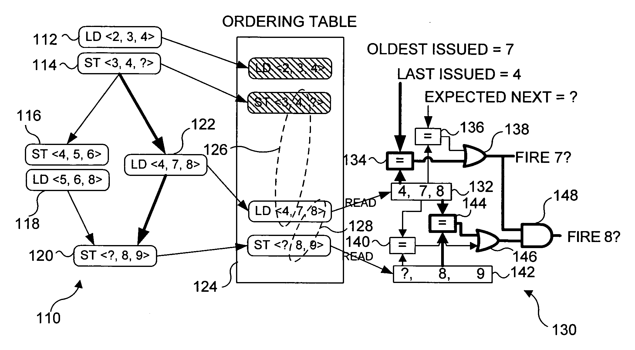
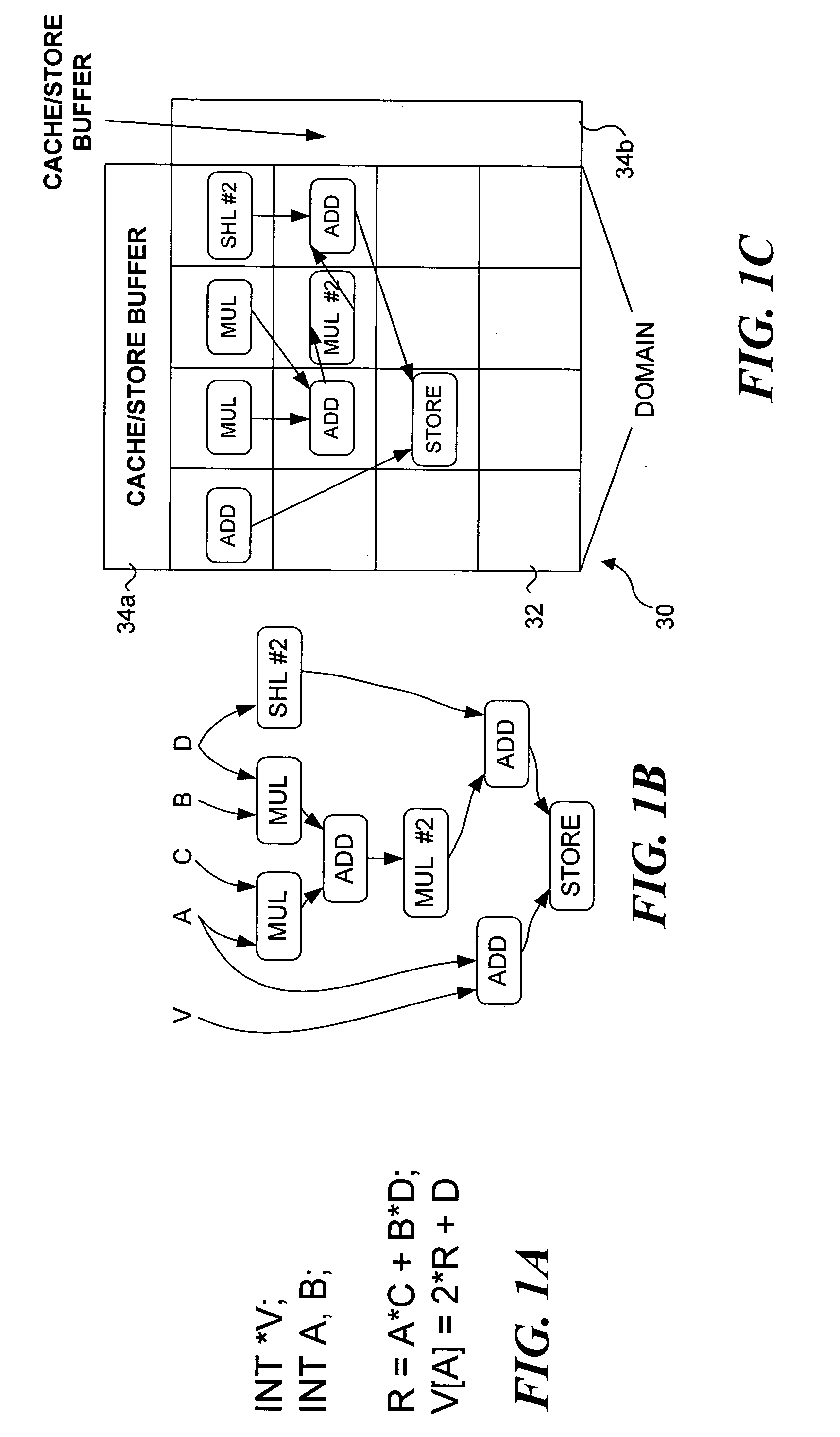
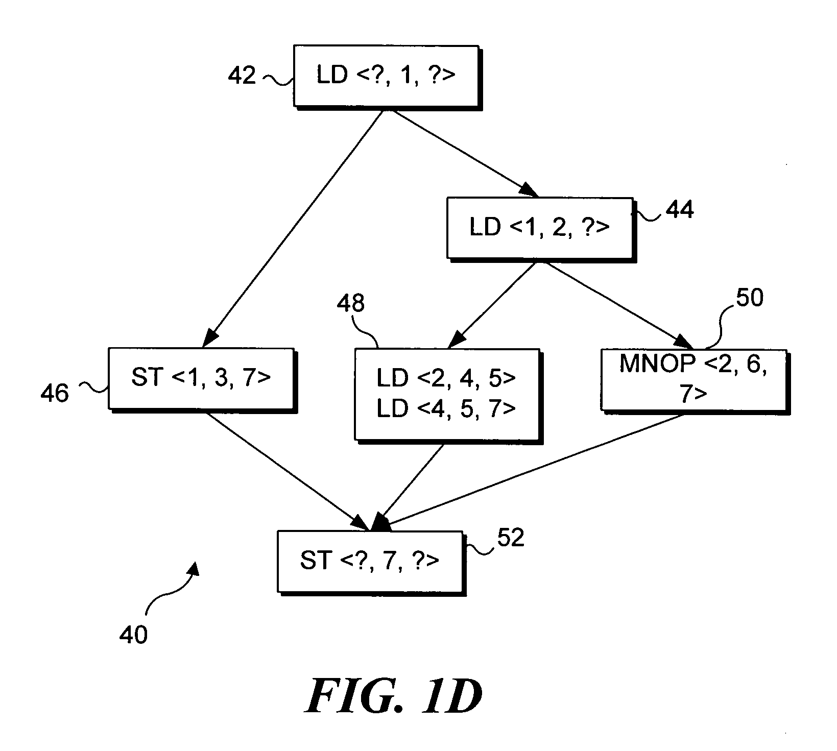
[0048] WaveScalar, a recently proposed architecture, is one example of the different ways being developed to convert silicon resources into application performance. Earlier WaveScalar work demonstrated its potential to outperform end-of-the-road superscalars and compete in the multithreaded design space. However, WaveScalar is a highly unusual design, utilizing hundreds of ALU cores and specialized and distributed memories. It might be appropriate to ask if WaveScalar can be built with current or even tomorrow's silicon technology? The following discussion addresses the buildability of WaveScalar's micro-architecture, which is referred to herein as the WaveCache. An RTL level design of the major WaveCache components is presented, and it includes: an execution core, a memory subsystem and a primary interconnect. Using a synthesizable implementation of this micro-architecture and a detailed instruction-level simulator, the area / performance trade-offs of alternative configurations of t...


PUM


Abstract

A dataflow instruction set architecture and execution model, referred to as WaveScalar, which is designed for scalable, low-complexity/high-performance processors, while efficiently providing traditional memory semantics through a mechanism called wave-ordered memory. Wave-ordered memory enables “real-world” programs, written in any language, to be run on the WaveScalar architecture, as well as any out-of-order execution unit. Because it is software-controlled, wave-ordered memory can be disabled to obtain greater parallelism. Wavescalar also includes a software-controlled tag management system.

Description

RELATED APPLICATIONS [0001] This application is based on a prior copending provisional application, Ser. No. 60 / 538,603, filed on Jan. 22, 2004, and on a prior copending provisional application, Ser. No. 60 / 630,765, filed on Nov. 24, 2004, the benefit of the filing dates of which is hereby claimed under 35 U.S.C. § 119(e).FIELD OF THE INVENTION [0002] The present invention generally pertains to a dataflow instruction set architecture (ISA) and execution model, and more specifically, to a dataflow ISA that includes many processors, each using a wave-ordered memory for executing instructions in waves, where the instructions are stored in distributed processor caches to minimize data transfer time. BACKGROUND OF THE INVENTION [0003] It is widely accepted that Moore's Law growth in available transistors will continue for the next decade. Recent research, however, has demonstrated that simply scaling up current architectures will not convert these new transistors to commensurate increase...

Claims


Application Information

Patent Timeline
IPC IPC(8): G06F15/00
CPCG06F9/3004G06F9/30087G06F9/3842G06F9/3851G06F9/4436G06F9/5016G06F2209/521G06F9/5038G06F9/52G06F9/522G06F9/526G06F15/8023G06F2209/5017G06F9/5033G06F9/4494
Inventor OSKIN, MARK H.SWANSON, STEVEN J.EGGERS, SUSAN J.
Owner UNIV OF WASHINGTON
Why Eureka
Try Eureka