

Power semiconductor device
a technology of semiconductor devices and semiconductors, applied in the direction of dc-ac conversion without reversal, process and machine control, instruments, etc., can solve the problems of increasing the load on the cpu, reducing the accuracy of measurement, and affecting the real time property, so as to achieve the effect of increasing the accuracy of measuremen
- Summary
- Abstract
- Description
- Claims
- Application Information
AI Technical Summary
Benefits of technology
Problems solved by technology
Method used
Image

Examples
first preferred embodiment
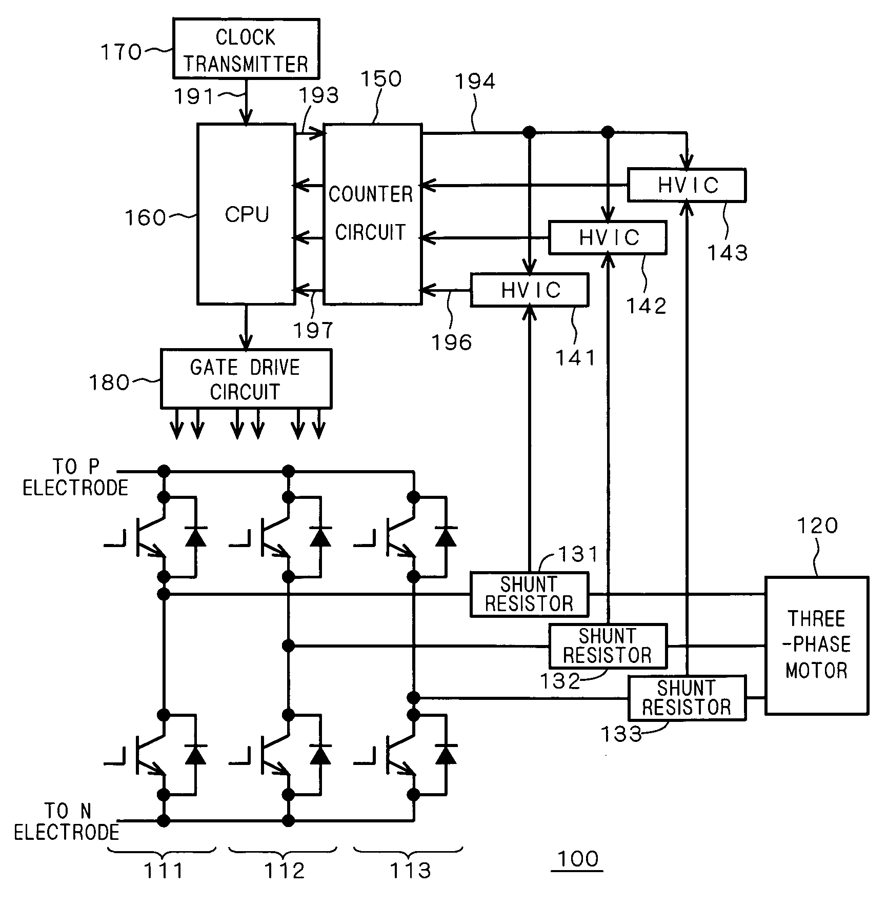
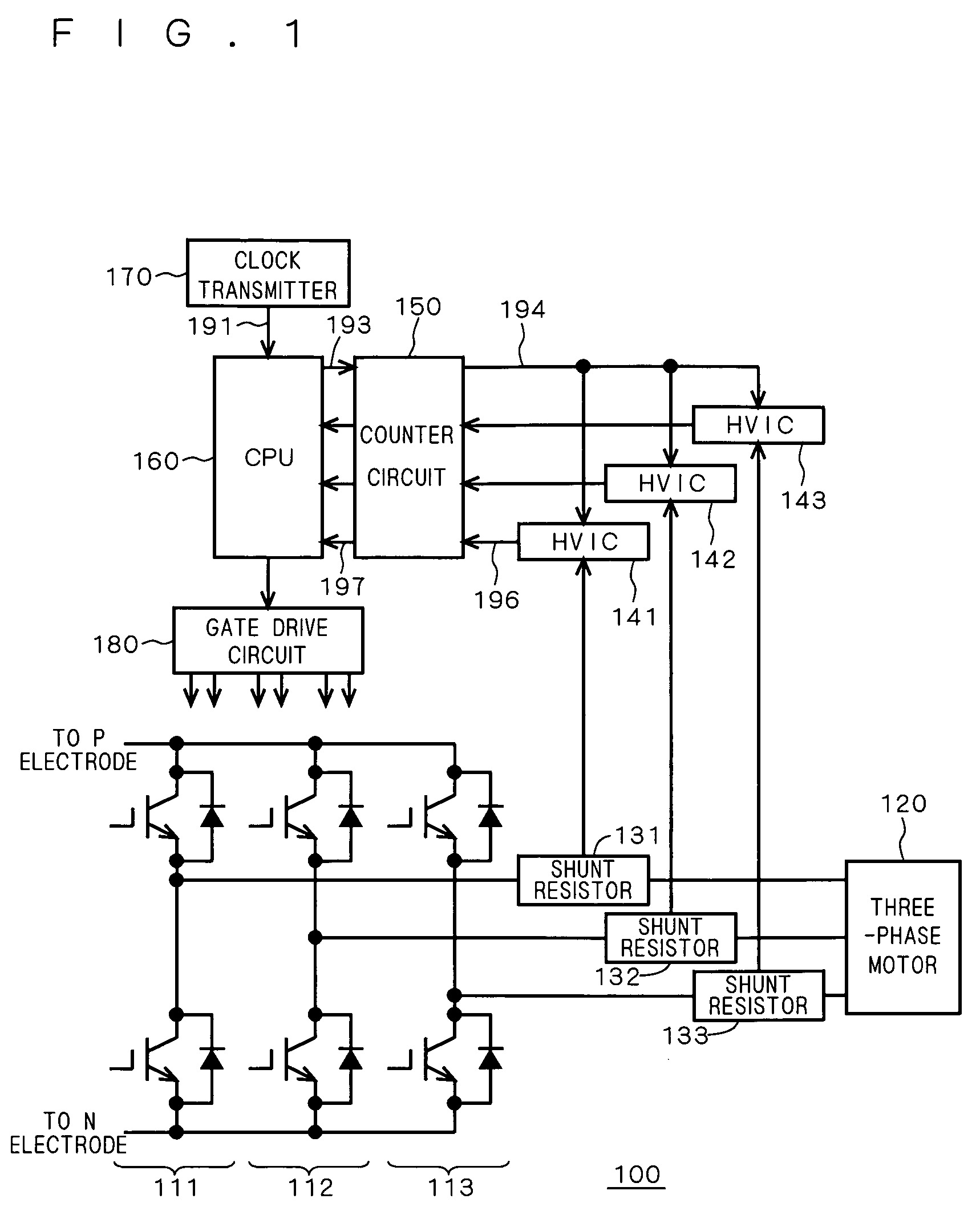
[0020]FIG. 1 shows the construction of a power semiconductor device 100 according to a first preferred embodiment of the present invention.
[0021] Referring to FIG. 1, inverter circuits 111 to 113 are connected to a P electrode and an N electrode, and supply current to the U, V and W phases, respectively, of a three-phase motor 120 to control the same. The inverter circuits 111 to 113 are connected to the three-phase motor 120 through shunt resistors 131 to 133, respectively. The shunt resistors 131 to 133 are connected to HVICs 141 to 143, respectively. The HVICs 141 to 143 are connected to a counter circuit 150. The counter circuit 150 is connected to a CPU 160. The CPU 160 is connected to a clock transmitter 170 and a gate drive circuit 180.
[0022] With reference to FIG. 1, voltages are developed across the respective shunt resistors 131 to 133, based on currents flowing to the U, V and W phases of the three-phase motor 120.
[0023] The operation of the power semiconductor device ...
second preferred embodiment
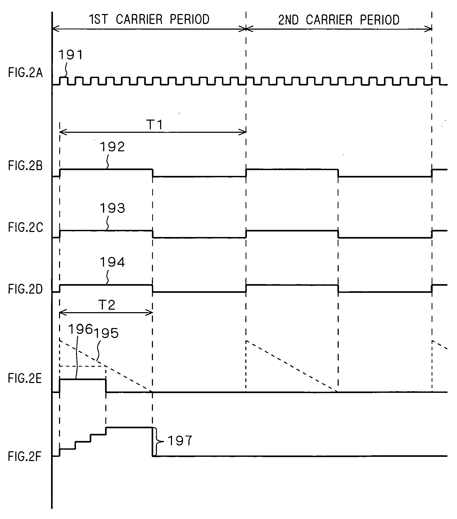
[0035] In the power semiconductor device 100 according to the first preferred embodiment, the counter circuit 150 inputs to the HVIC 141 the second synchronization signal 194 the delay time of which is zero from the first synchronization signal 193, as shown in FIG. 2D. The counter circuit 150, however, may delay the input of the second synchronization signal 194 to the HVIC 141 by delay time T3 from the first synchronization signal 193. The delay time T3 is obtained by subtracting the width T2 of the inverted sawtooth signal 195 and processing time T4 in the counter circuit 150 from the period T1 of the carrier signal 192 (i.e., T3=T1−T2−T4). The processing time T4 is the time required for processing in the counter circuit 150 between the completion of the counting and the output of the numerical data 197.
[0036]FIGS. 3A to 3F are timing charts showing the operation of the power semiconductor device according to a second preferred embodiment of the present invention. FIGS. 3A to 3F...
third preferred embodiment
[0039] In general, the period T1 of the carrier signal 192 differs depending on the various constituents to be controlled, such as the three-phase motor 120 and the inverter circuits 111 to 113. Further, if problems (including noise, heat generation, quality variation of parts and the like) not assumed in the early stages of development have surfaced, it is necessary to change the delay time T3. This creates the need to develop power semiconductor devices for each type of automotive vehicles on which the power semiconductor devices are to be mounted, and a problem such that the development period for the power semiconductor devices might be prolonged.
[0040]FIG. 4 shows the construction of a power semiconductor device 101 according to a third preferred embodiment of the present invention. The power semiconductor device 101 shown in FIG. 4 includes a counter circuit 152 constituted by CPLD (Complex Programmable Logic Devices) and the like and having an interface 153, in place of the ...
PUM
 Abstract
Description
Claims
Application Information