Semiconductor device with a metal insulator semiconductor transistor

a semiconductor transistor and semiconductor technology, applied in semiconductor devices, digital storage, instruments, etc., can solve the problem of hardening the multibit information in one memory cell as the scaling progresses, and achieve the effect of increasing the effective channel length

Inactive Publication Date: 2005-08-04
RENESAS TECH CORP
View PDF10 Cites 5 Cited by
  • Summary
  • Abstract
  • Description
  • Claims
  • Application Information

AI Technical Summary

Benefits of technology

[0025] In the MIS transistor, the gate electrode is formed on the gate insulating film to enter the trench. The first and second electric charge holding portions are formed in the gate insulating film to interpose the trench therebetween. In the case in which an electric charge is trapped into the first electric charge holding portion and another electric charge is then trapped into the second electric charge holding portion, accordingly, the gate electrode in the trench functions as a shield. More specifically, the second electric charge holding portion is not influenced by an electric field induced by the electric charge of the first electric charge holding portion, and the trapping of the electric charge into the second electric charge holding portion is not inhibited even if scaling progresses. If the MIS transistor is applied to a memory cell of a nonvolatile memory, therefore, a semiconductor device capable of holding multibit information in one memory cell can be implemented also when scaling for the nonvolatile memory progresses. Moreover, the trench is formed between the source region and the drain region. Consequently, an effective channel length can be increased and a tolerance to a punch-through can also be enhanced.

Problems solved by technology

With a structure of a conventional semiconductor device, therefore, it is harder to hold multibit information in one memory cell when the scaling progresses.

Method used


Image

  • Semiconductor device with a metal insulator semiconductor transistor
  • Semiconductor device with a metal insulator semiconductor transistor
  • Semiconductor device with a metal insulator semiconductor transistor

Examples


first embodiment

[0061] The present embodiment provides a semiconductor device comprising an MONOS transistor having such a structure that a trench is formed in a channel portion and a silicon nitride film in a gate insulating film is formed as an electric charge holding portion to interpose the trench.

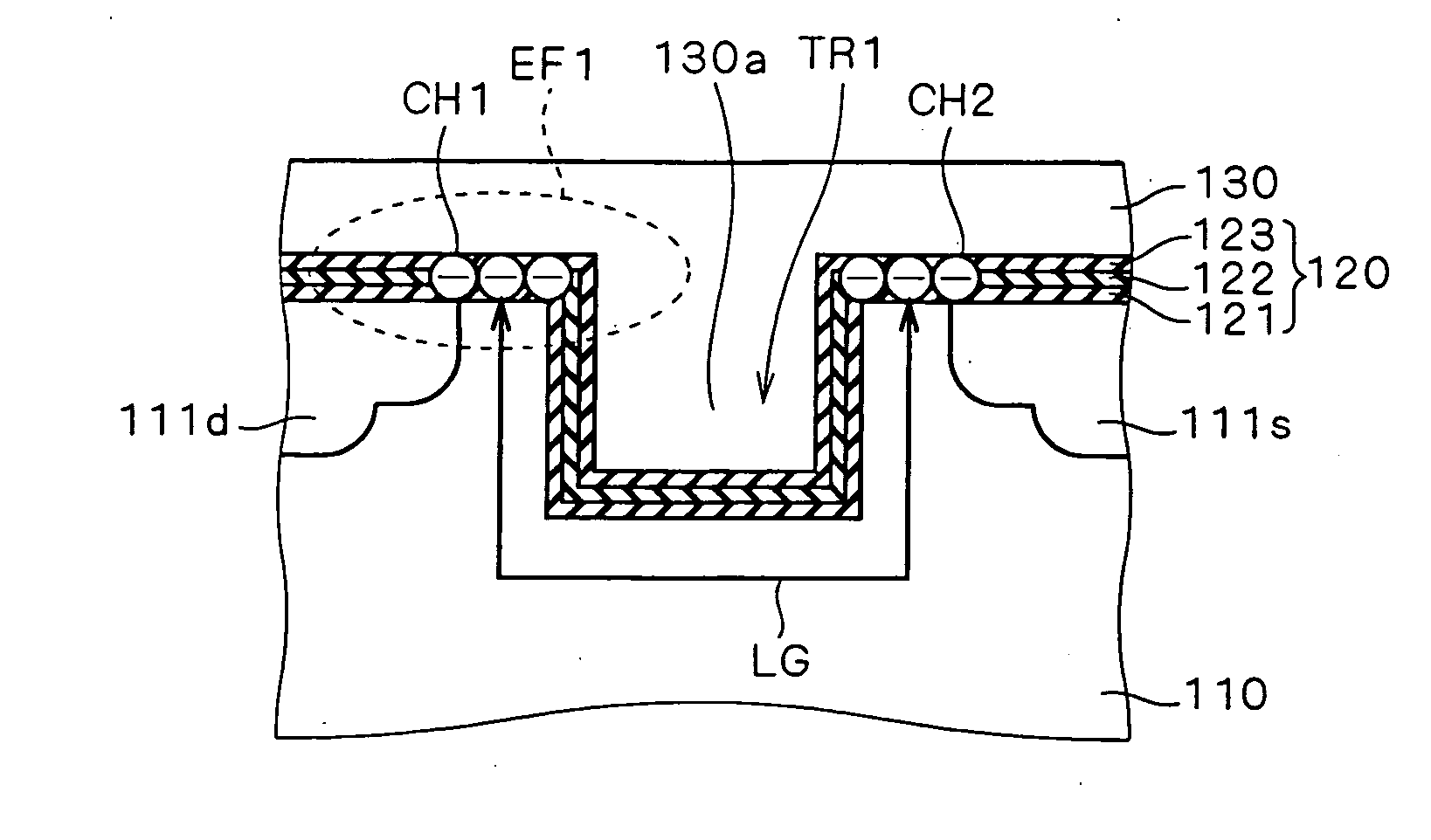
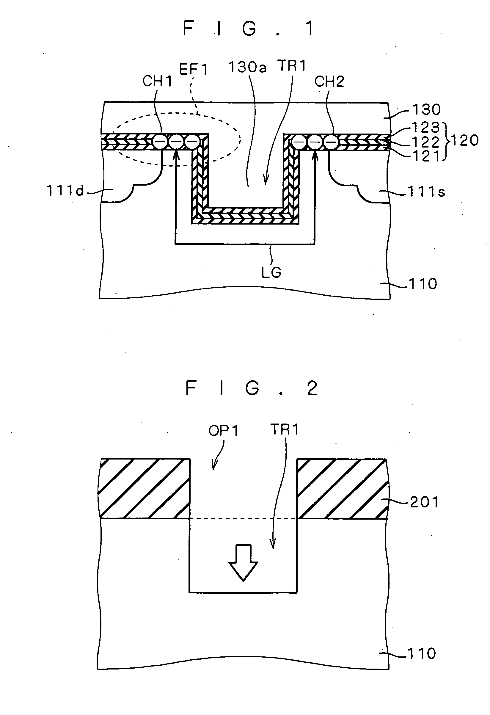
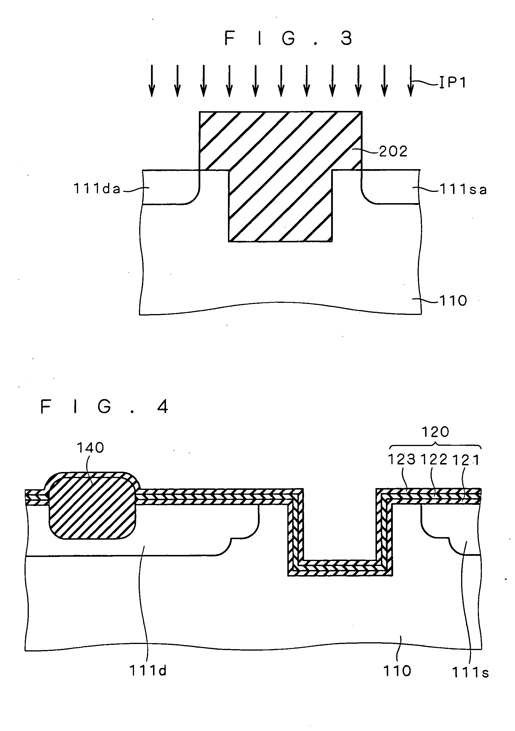
[0062]FIG. 1 is a view showing an MONOS transistor provided in a semiconductor device according to the present embodiment. As shown in FIG. 1, the MONOS transistor comprises a source region 111s and a drain region 111d which are formed in a semiconductor substrate 110 such as a silicon substrate, a gate insulating film 120 formed on the semiconductor substrate 110, and a gate electrode 130 formed on the gate insulating film 120. The gate insulating film 120 is a laminated film in which a silicon oxide film 121, a silicon nitride film 122 and a silicon oxide film 123 are sequentially provided.

[0063] In the present embodiment, a trench TR1 is formed in a channel portion between the source region 111s ...

second embodiment

[0069] The present embodiment is an example of a method of manufacturing the semiconductor device according to the first embodiment.

[0070] First of all, as shown in FIG. 2, a mask 201 such as a photoresist, a silicon oxide film or a silicon nitride film is formed on a semiconductor substrate 110, and an opening OP1 is provided therein so that a trench TR1 is formed on a surface of the semiconductor substrate 110 by anisotropic etching.

[0071] Next, well formation, channel doping and the like are carried out. As shown in FIG. 3, then, a mask 202 such as a photoresist is formed and LDD (Lightly Doped Drain) regions 111sa and 111da are formed by an impurity implantation IP1 in positions facing the surface of the semiconductor substrate 110 with the trench TR1 interposed therebetween. In the same manner, thereafter, an impurity is implanted in a higher concentration than that of each of the LDD regions 111sa and 111da to form a source region 111s and a drain region 111d.

[0072] Subsequ...

third embodiment

[0093] The present embodiment is another example of the method of manufacturing the semiconductor device according to the first embodiment.

[0094] First of all, a dummy film (for example, a silicon oxide film) 203 is formed on a semiconductor substrate 110 and a first mask film (for example, a silicon nitride film) 204 having an etching selectivity for the dummy film 203 is further formed on the dummy film 203 (FIG. 5). The reason why (120) is attached to the designation of the dummy film 203 in FIGS. 5 to 13 is that these drawings are also used in a seventh embodiment. In the present embodiment, a portion having (120) attached thereto can be disregarded.

[0095] Next, a photoresist 205 is formed and is then patterned to provide an opening OP2 (FIG. 6). Thereafter, anisotropic etching is carried out over the dummy film 203 and the first mask film 204. Consequently, an opening is formed in a region AR1 in which an isolating region is to be formed (FIG. 7).

[0096] Subsequently, the pho...


PUM


Abstract

It is an object to provide a semiconductor device capable of holding multibit information in one memory cell also when scaling for a nonvolatile memory progresses, and a method of manufacturing the semiconductor device. A trench (TR1) is formed in a channel portion of an MONOS transistor. Then, a source side portion and a drain side portion in a silicon nitride film (122) of a gate insulating film (120) which interpose the trench (TR1) are caused to function as first and second electric charge holding portions capable of holding electric charges (CH1) and (CH2). In the case in which the electric charges (CH1) are trapped and the electric charges (CH2) are then trapped, thus, a portion (130a) of a gate electrode (130) in the trench (TR1) functions as a shield. If a fixed potential is given to the gate electrode (130), the second electric charge holding portion is not influenced by an electric field (EF1) induced by the electric charges (CH1) so that the trapping of the electric charges (CH2) is not inhibited.

Description

BACKGROUND OF THE INVENTION [0001] 1. Field of the Invention [0002] The present invention relates to a semiconductor device to be utilized for a memory cell of a nonvolatile memory and a method of manufacturing the semiconductor device. [0003] 2. Description of the Background Art [0004] Examples of a semiconductor device to be utilized for a memory cell of a nonvolatile memory include an MONOS (Metal Oxide Nitride Oxide Semiconductor) transistor having a structure shown in FIG. 35. The MONOS transistor comprises a source region 111s and a drain region 111d which are formed in a semiconductor substrate 110, a gate insulating film 120 formed on the semiconductor substrate 110, and a gate electrode 130 formed on the gate insulating film 120. [0005] The gate insulating film 120 is a laminated film (an ONO film) in which a silicon oxide film 121, a silicon nitride film 122 and a silicon oxide film 123 are sequentially provided. When the MONOS transistor is to be under a programming (writ...

Claims


Application Information

Patent Timeline
Patent Type & Authority Applications(United States)
IPC IPC(8): H01L21/28H01L21/8247H01L21/336H01L27/115H01L29/788H01L29/792
CPCH01L21/26586H01L21/28282H01L27/115H01L27/11568H01L29/42352H01L29/7923H01L29/513H01L29/66545H01L29/66583H01L29/66833H01L29/7833H01L29/42368H01L29/40117H10B69/00H10B43/30
Inventor ITOH, YASUYOSHIUENO, SHUUICHIFURUTA, HARUOAJIKA, NATSUO
Owner RENESAS TECH CORP
Why Eureka
Try Eureka