Method of producing printed circuit board with embedded resistor

a technology of embedded resistors and printed circuit boards, which is applied in the direction of resistor housing/enclosement/embedding, printing, metallic pattern materials, etc., can solve the problems of not being able to directly apply resin-based substrates, and 594 is applied to only ceramic substrates. achieve the effect of improving workability

Inactive Publication Date: 2005-08-11
SAMSUNG ELECTRO MECHANICS CO LTD
View PDF4 Cites 38 Cited by
  • Summary
  • Abstract
  • Description
  • Claims
  • Application Information

AI Technical Summary

Benefits of technology

[0026] Accordingly, the present invention has been made keeping in mind the above problems occurring in the prior art, and an aspect of the present invention is to provide a method of producing a PCB with an embedded

Problems solved by technology

However, the chip resistors are disadvantageous in that it is difficult to apply the discrete chip resistors to light and small electronic parts, and the discrete chip resistors occupy a relatively large area.
However, the '594 is applied to only a ceramic substrate, but cannot be directly applied to a resin-based substrate, for example, a substrate made of epoxy-glass or polyimide.
However, the above patents are disadvantageous in terms of predictability and tolerance limitation of a resistance value of the resistor.
On the other hand, in the case of using the substrate made of a plastic material with a large area, it is difficult to secure the precision in the laser trimming process and to practically apply the laser trimming process to the PCB because the resistance value is changed by heat due to a laser beam, and operation costs are high.
However, in the case of the exterior-type process, the copper terminations 2, 2′ exposed to external environments may be readily oxidized because of a process delay between the second and third step.
However, the small resistance value disturbs the mass production of the PCB.
Accordingly, when the resistor paste is coated on the resin-based substrate, it is non-uniformly coated on the substrate, and a non-uniform thickness of the resistor paste lead

Method used


Image

  • Method of producing printed circuit board with embedded resistor
  • Method of producing printed circuit board with embedded resistor
  • Method of producing printed circuit board with embedded resistor

Examples


first embodiment

[0063]FIGS. 2A to 2D are sectional views illustrating the production of a PCB with an embedded resistor according to the present invention.

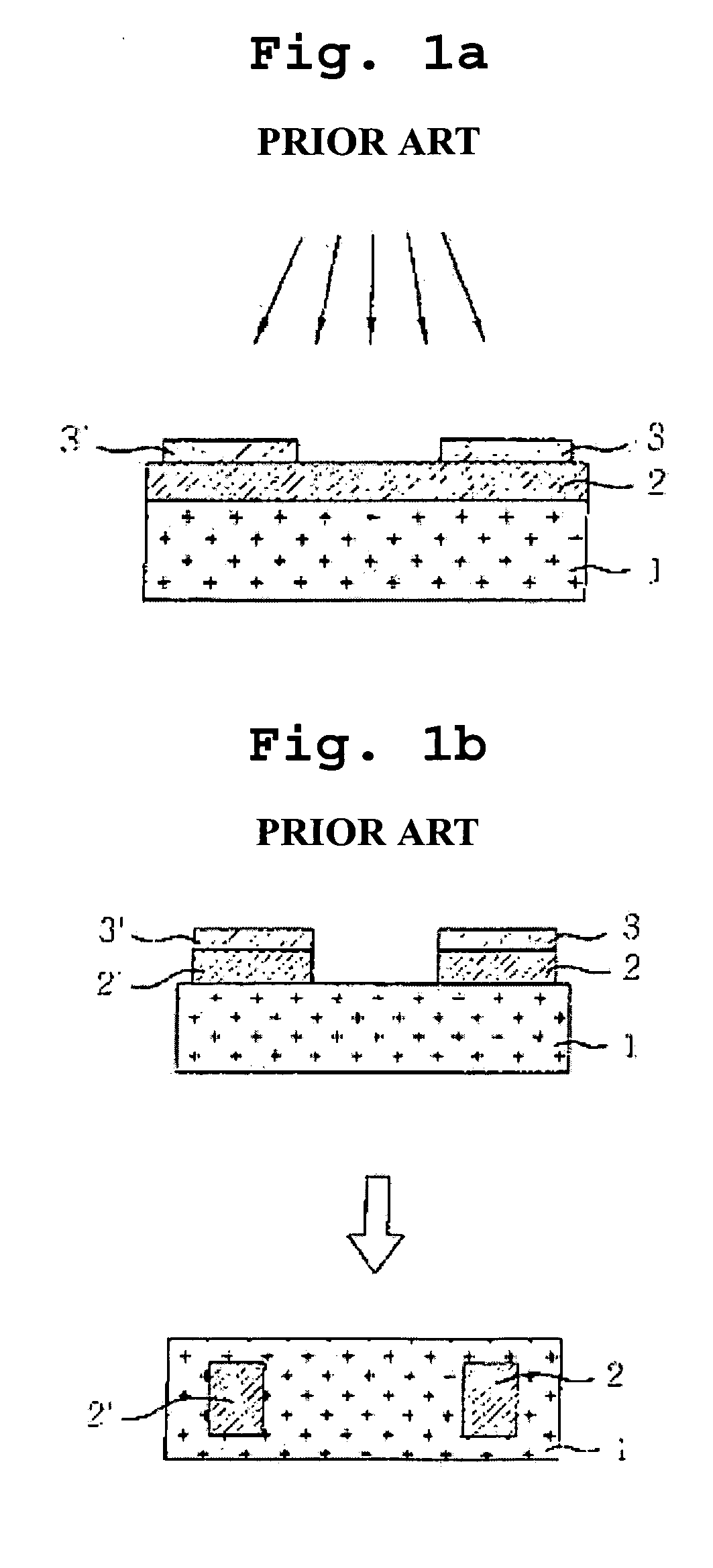
[0064] With reference to FIG. 2A, there is illustrated a sectional view of a copper clad laminate 21 used as a base substrate. The copper clad laminate 21 is a thin laminate composed of a reinforcing base substrate 23 and a copper clad 22 coated on the reinforcing base substrate 23. Various kinds of copper clad laminates may be used to produce the PCB, but in the present invention, a FR-4 copper clad laminate, a resin-coated PCB in which a copper clad is coated on a reinforcing base substrate composed of a glass fiber added by an epoxy resin, is sufficiently competitive in terms of production costs of the copper clad laminate.

[0065] An etching resist is coated on the copper clad 22 of the copper clad laminate 21, exposed, and developed using a mask film on which a resistor paste pattern is printed to form an etching resist pattern on the copper ...

second embodiment

[0079] Referring to FIGS. 6A to 6E, after the resistor paste 66 is ground as shown in FIG. 2D or 3C, a copper plated layer is additionally layered on a copper clad 62 and resistor paste 66, and a circuit pattern is then formed on a copper clad laminate 61 according to the present invention.

[0080]FIG. 6A is a sectional view of a copper clad laminate 61 used as a base substrate. The copper clad laminate 61 is a thin laminate composed of a reinforcing base substrate 63 and the copper clad 62 coated on the reinforcing base substrate 63. Various kinds of copper clad laminates may be used to produce a PCB, but in the present invention, it is preferable to use a FR-4 copper clad laminate in which a copper clad is coated on a reinforcing base substrate composed of a glass fiber added by an epoxy resin.

[0081] With reference to FIG. 6B, an etching resist pattern is formed on a portion of the copper clad 62 on the copper clad laminate 61, corresponding to a space 64 to be filled with a resist...

third embodiment

[0090] According to the present invention, as shown in FIGS. 8A to 8H, after a plating resist pattern 84 is formed on a portion of a copper clad 82 corresponding to a space to be filled with a resistor paste 88 so as to prevent such portion of the copper clad 82 from being plated with a metal, the copper clad laminate 81 is then plated with the metal. An etching resist is selectively formed on the copper clad laminate 81 plated with the metal, the plating resist pattern 84 is removed from the copper clad laminate 81, a portion of the copper clad 82 corresponding to the space to be filled with the resistor paste 88 is etched and removed, and the resistor paste 88 is filled in a space formed by the copper clad 82, a copper plated layer 85, and the copper clad laminate 81, thereby forming a resistor on the copper clad laminate 81.

[0091]FIG. 8A is a sectional view of the copper clad laminate 81 used as a base substrate. The copper clad laminate 81 is a thin laminate composed of a reinfo...


PUM

PropertyMeasurementUnit
Thicknessaaaaaaaaaa
Electrical conductivityaaaaaaaaaa

Abstract

Disclosed is a method of producing a printed circuit board (PCB) with an embedded resistor, in which a resistor with a desired shape and volume is precisely formed using a resistor paste so that resistance values according to a position of the PCB are uniform, thereby a laser trimming process is omitted or minimally utilized. The method has advantages in that a production time of the PCB is shortened and productivity is improved because an operation condition is rapidly set without being greatly affected by the position precision of a printing device. Other advantages of the method are that the resistor paste with a relatively uniform thickness is secured through a screen printing process, thereby easily forming the resistor and improving resistance tolerance.

Description

FIELD OF THE INVENTION [0001] The present invention pertains to a method of producing a printed circuit board (PCB) with an embedded resistor. More particularly, the present invention relates to a method of producing a PCB with an embedded resistor, in which a resistor with a desired shape and volume is precisely formed using a resistor paste so that resistance values according to a position of the PCB are uniform, thereby a laser trimming process is omitted or minimally utilized. Accordingly, the method has advantages in that a production time of the PCB is shortened and productivity is improved because an operation condition is rapidly set without being greatly affected by the position precision of a printing device. Other advantages of the method are that the resistor paste with a relatively uniform thickness is secured through a screen printing process, thereby easily forming the resistor and improving resistance tolerance. DESCRIPTION OF THE RELATED ART [0002] Generally, a PCB ...

Claims


Application Information

Patent Timeline
IPC IPC(8): H01L23/12H05K1/09H05K1/16H05K3/30H05K3/06H05K3/10
CPCB23K26/0003Y10T29/49101H05K1/095H05K1/167H05K3/064H05K3/108H05K2201/0347H05K2203/1461Y10T29/49098Y10T29/49082Y10T29/49126Y10T29/49151Y10T29/4913Y10T29/49156B23K2201/42B23K26/351B23K2101/42H05K3/30
Inventor CHO, SUK-HYUNKANG, JANG-KYUSUN, BYUNG-KOOKHONG, JONG-KUKLEE, SEOK-KYUAHN, JIN-YONG
Owner SAMSUNG ELECTRO MECHANICS CO LTD
Why Eureka
Try Eureka