However, such contemporary reactors suffer from inherent deficiencies which detract from their overall desirability, particularly with respect to
high pressure and / or high temperature CVD processes.
When using the aforementioned reactor designs under
high pressure and temperature conditions, heavy thermal
convection inherently occurs.
Such thermal
convection undesirably interferes with the growth process, so as to degrade efficiency and yield.
Thermal
convection is detrimental to growing high quality thin films since hard-to-control complex chemical reactions occur due to the extended duration of the presence of reactant gases in the growth chamber.
This inherently results in a decrease in growth efficiency and poor film uniformity.
This high consumption of
ammonia results in the corresponding high costs.
Reaction between source chemicals in the
gas phase is another important issue in the contemporary MOCVD process for growth of GaN.
However, it is not avoidable in the group III
nitride MOCVD process because the reaction is severe and fast.
When the group III alkyls (such as
trimethylgallium,
trimethylindium, trimethylaluminum) encounter ammonia, a reaction occurs almost immediately, resulting in the undesirable formation of adducts
This process will eventually deplete the sources, thereby making the growth process undesirably vary between runs and / or will clog the gas entrance.
An efficient
reactor design for III-
nitride growth does not avoid
gas phase reaction, but rather controls the reaction so that it does not create such undesirable situations.
However, when a reactor is scaled up this way, several new issues arise.
Because thermal convection is as severe (or even more sever) in a larger reactor as in a smaller reactor, film uniformity, as well as
wafer-to-
wafer uniformity, are not any better (and may be much worse).
Further, at higher growth pressures, a very high gas flow rate is needed to suppress thermal convection.
Additionally, because of the high temperature requirements, the larger mechanical parts of such a scaled up (larger) reactor are inherently placed under higher thermal stress and consequently tend to break prematurely.
Because of hydrogenation of the metals utilized (making them become brittle) and because of
etching of
graphite by ammonia at high temperatures, the larger
metal and
graphite parts tend to break down much sooner than the corresponding parts of smaller reactors.
Larger
quartz parts also become more susceptible to breakage because higher thermal stress.
Another issue associated with
large size reactors is the difficulty in maintaining high temperature uniformity.
The reliability of the heater
assembly is usually poor due to the aforementioned high thermal stress and ammonia degradation.
These issues of process inconsistency and extensive hardware maintenance have a significant
impact on production yield and therefore product cost.
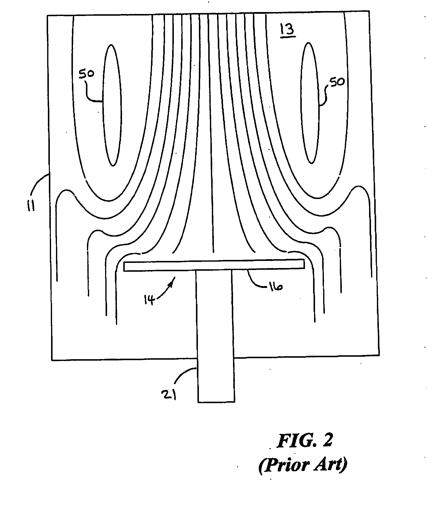
However, when growing GaN at high pressures and temperatures in a high ammonia ambient gas, then thermal convection occurs and gas flow tends to be undesirably turbulent.
It is clear that turbulence increase as the size of the chamber and / or the distance between the wafer carrier and the top of the chamber increases.
As those skilled in the art will appreciate, such recirculation is undesirable because it results in undesirable variations in reactant concentration and temperature.
Further, such recirculation generally results in reduced growth efficiency due to ineffective use of the reactant gas.
This, of course, undesirably complicates the construction of such larger reactors and increases the cost thereof.
From this comparison, it is clear that such scaling up of a reactor to accommodate more wafers greatly increases the size, particularly the volume, thereof.
This increase in the size of the reactor results in the undesirable effects of thermal convection and the additional complexities of construction discussed above.
It is well known, however, that the depletion effect is one major drawback in contemporary horizontal reactors.
This undesirably makes the thin film deposited thinner and thinner along the radial direction upon the wafer.
The drawback of this approach is an inherent decrease in growth efficiency.

