Structure of a circuit board for improving the performance of routing traces

a circuit board and routing trace technology, applied in the direction of printed circuit aspects, high frequency circuit adaptations, metallic pattern materials, etc., can solve the problems of severe elimination of the performance and frequency response of routing trace in a pcb, complicated circuit board design, and resonant effect, so as to improve the performance of routing trace, eliminate the resonant effect, and improve the effect of routing trace respons

Active Publication Date: 2005-08-18
VIA TECH INC
View PDF11 Cites 5 Cited by
  • Summary
  • Abstract
  • Description
  • Claims
  • Application Information

AI Technical Summary

Benefits of technology

[0010] Broadly speaking, the present invention discloses a structure of a circuit board for improving performance of the routing traces, which are used to eliminate the resonant effect from the layers of the circuit board and improve the routing trace response.

Problems solved by technology

As a result, the design of the circuit board is more complicated and concentrated, and a multi-layer circuit board with area reduction is in development.
The problem of voltage variation may occur when the current passes through the IC to induce a voltage drop.
The negative effect of a stray capacitor produced among these planes will severely eliminate the performance and frequency response of routing trace in a PCB.
It is apparent that there is a large-amplitude resonance occurring at 3.9 Ghz, as shown in the diagram, and this will decrease the quality of the circuit structure.

Method used


Image

  • Structure of a circuit board for improving the performance of routing traces
  • Structure of a circuit board for improving the performance of routing traces
  • Structure of a circuit board for improving the performance of routing traces

Examples


first embodiment

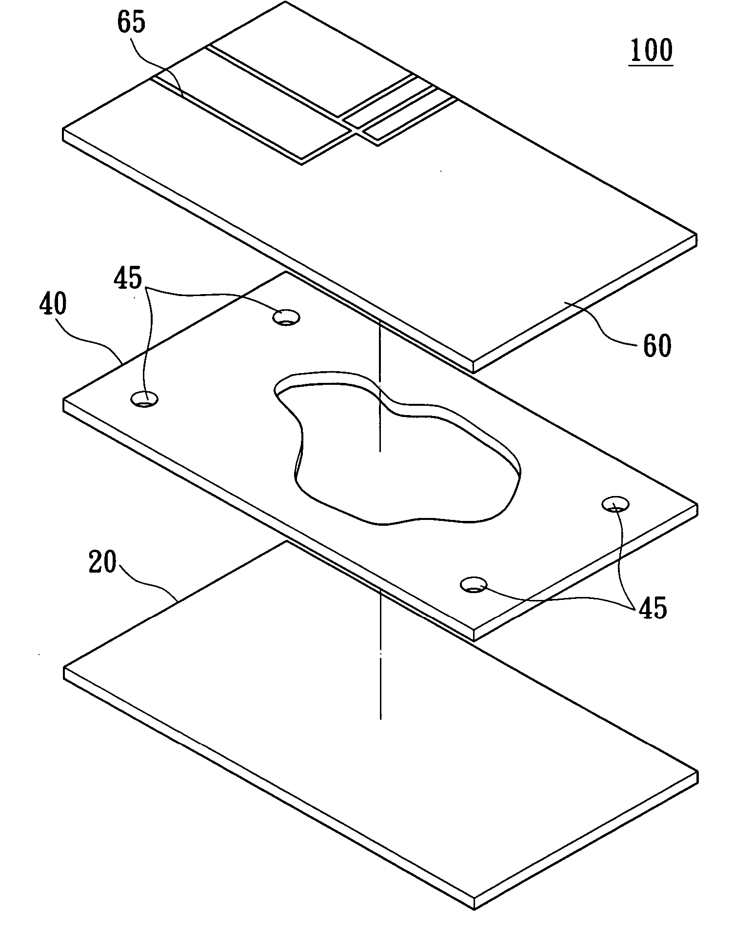
[0027]FIG. 4 shows the structure of a circuit board 100 in the present invention. The etching hole 50 shown in this drawing covers the above routing trace 65 entirely, in which the routing trace 65 is made of metal fine trace, whose width can be designed or the thickness of electric layer of routing trace 65 can be increased as the characteristic impedance requires. Moreover, the size of area of the etching hole 50 next to the routing plane 60 also can be designed to or not to link with the via hole 45, and the routing plane 60 can connect to the power plane 40 and ground plane 20 via conductive plugs inside these via hole 45. Accordingly, to provide a better frequency response, the invention provides different embodiments for any specific case.

[0028] Since the area of the routing trace on a circuit board is insufficient, the other routing traces should set on the other side or the inner layer of the circuit board as are the six layers shown in FIG. 5, which illustrates the second e...

third embodiment

[0029] the circuit board structure in the present invention is illustrated in FIG. 6. There are probably many power sets with different voltages on power plane, and which are divided into the first power plane 61 and second power plane 62 shown in FIG. 6 by one or a plurality of etching slots 63, especially in the manufacturing process of microchip. Several power sets including first power plane 61 and second power plane 62 on power plane are divided by etching slot 63 with any shape, so the routing trace 64 in the under layer can make electric potential reference to the ground plane. In practice, the width of the etching slot 63 is not five times smaller than the width of the routing trace 64.

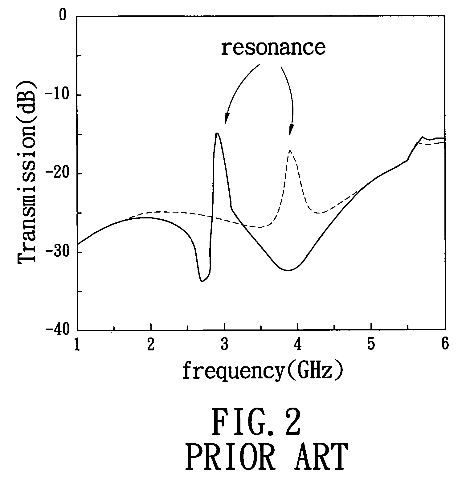
[0030] The schematic diagram of the experimental results of the frequency response is shown in FIG. 7, which shows the smoother curve around the previous peaks of 2.9 GHz and 3.9 GHz. It shows the result of effectively reducing the resonance effect and parasitic resonance in the prior art. The...


PUM


Abstract

A structure of a circuit board for improving the performance of routing traces is described as eliminating the resonant effects from the inner layers in a circuit board. For eliminating the stray capacitor effect between the planes in the circuit board, the present invention uses a method for etching an area of a power plane and the area is corresponding to a routing plane. Consequently, the routing trace can make good electric potential reference of a ground plane. Due to the reduction of the stray capacitor, the structure for improving the performance of routing traces of the invention can avoid the resonance effect and parasitic resonance in the circuit board as produced in a high-frequency situation in order to promote the quality of the circuit board.

Description

BACKGROUND OF THE INVENTION [0001] 1. Field of the Invention [0002] The present invention relates to a structure of a circuit board with an etching hole or slot in the power plane for eliminating the resonance effect and parasitic resonance on each trace. [0003] 2. Description of Related Art [0004] A printed circuit board (PCB) is a circuit system with some specific functions and connected to a plurality of electronic elements like those in the telecommunications, high-frequency circuits, communication systems, aviation, ships, appliances, cars, machines and all kinds of instruments. For the technique advancement of IC, in which more conducting pins are required, the more complicated routing traces are also needed. As a result, the design of the circuit board is more complicated and concentrated, and a multi-layer circuit board with area reduction is in development. [0005] The method for manufacturing the conventional PCB is to press a plurality of layers with different functions, i...

Claims


Application Information

Patent Timeline
Patent Type & Authority Applications(United States)
IPC IPC(8): H05K1/02
CPCH05K1/0253H05K2201/093H05K1/0262H05K2201/0969H05K2201/09663
Inventor LEE, SHENG-YUAN
Owner VIA TECH INC
Why Eureka
Try Eureka