Method to form a contact hole

a contact hole and etching technology, applied in the manufacturing of semiconductor/solid-state devices, basic electric elements, electric devices, etc., to achieve the effect of reducing repetition

Inactive Publication Date: 2005-08-18
TAIWAN SEMICON MFG CO LTD
View PDF4 Cites 249 Cited by
  • Summary
  • Abstract
  • Description
  • Claims
  • Application Information

AI Technical Summary

Benefits of technology

[0014] The above advantages and features are of representative embodiments only, and are not exhaustive and/or exclusive. They are presented only to assist in understanding the invention. It should be understood that they are not representative of all the inventions defined by the claims, to be considered limitations on the invention as defined by the claims, or limitations on equivalents to the claims. For instance, some of these advantages may be mutually contradictory, in that they cannot be simultaneously present in a single embodiment. Similarly, some advantages are

Problems solved by technology

For instance, some of these advantages may be mutually contradictory,

Method used


Image

  • Method to form a contact hole
  • Method to form a contact hole
  • Method to form a contact hole

Examples


Embodiment Construction

I. Overview of an Aspect of the Invention

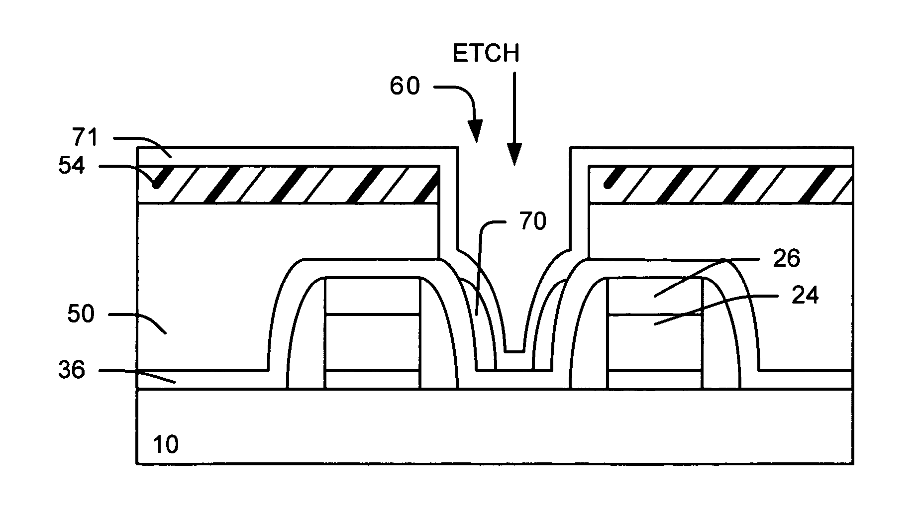
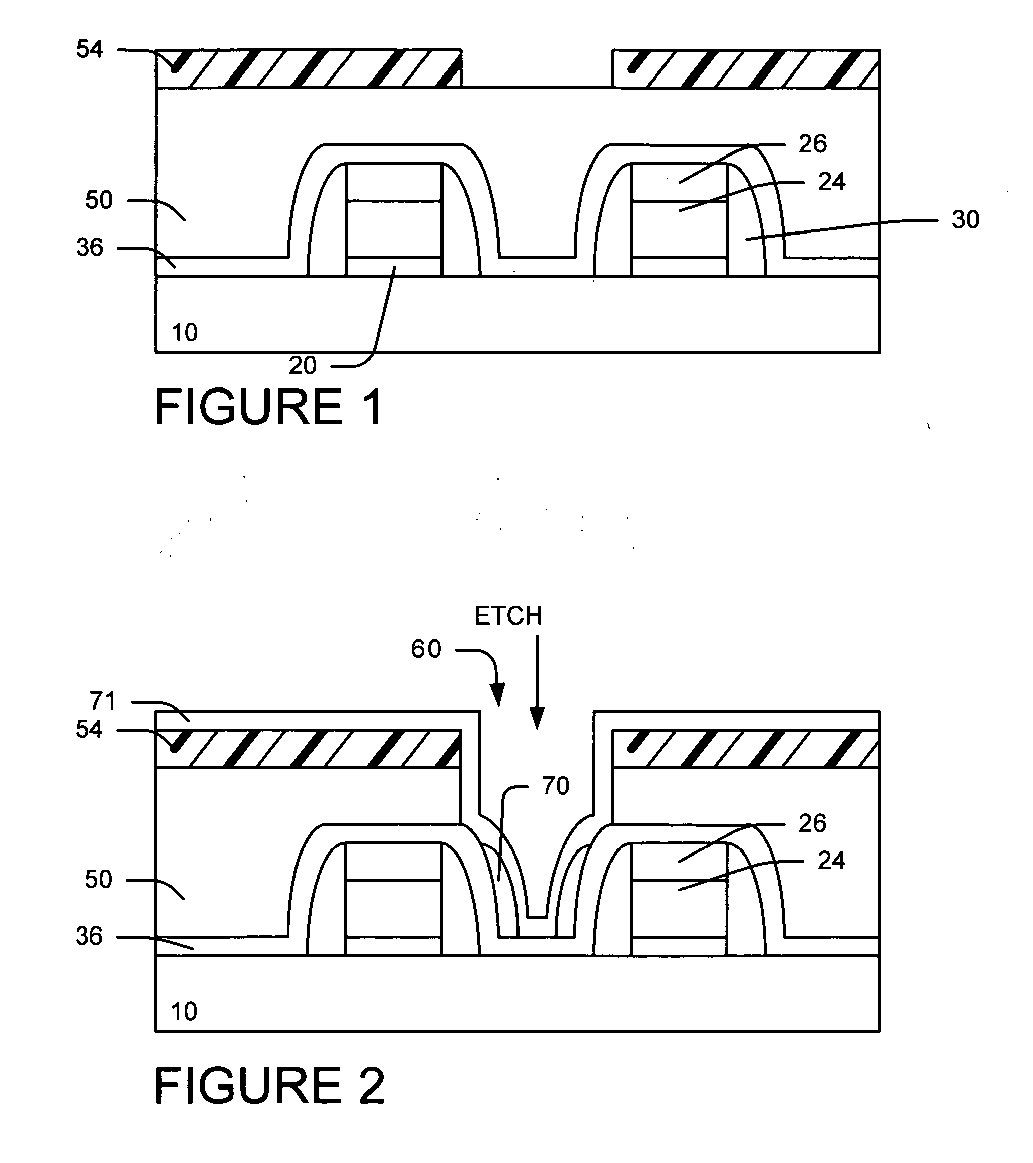
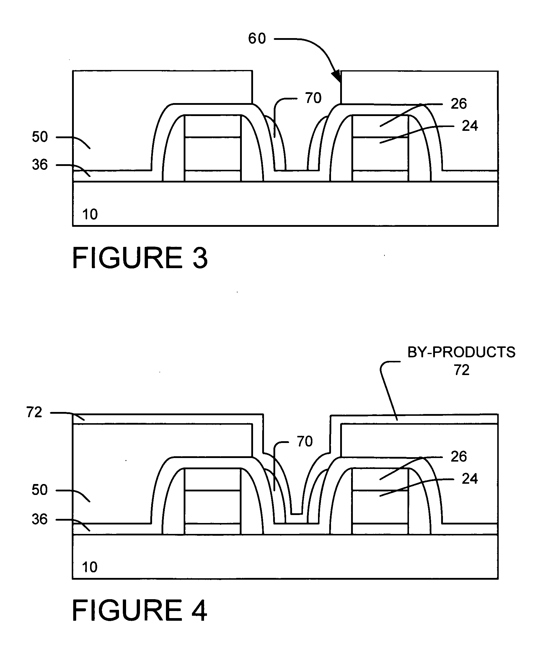
[0022] Embodiments show a method for removing a residue oxide spacer from a contact opening sidewall. A contact opening is etched into a dielectric layer comprised of oxide. The etch process creates an undesired residual oxide spacer on the contact opening sidewall. (See FIG. 3, residual spacer 70) A plasma treatment using nitrogen, fluorine and hydrogen containing gasses (e.g., NF3 and N2+H2) is used to form a by-products layer over the undesired residual oxide spacer. (See FIG. 4, by-products layer 72) Then the by-products layer and the undesired residual oxide spacer are preferably removed using one of the following: (1) heating, (2) DI rinse and (3) UV radiation. See FIG. 5.

II. Method to an Opening

[0023] Embodiments of present invention will be described in detail with reference to the accompanying drawings. Some embodiments provide a method of forming a contact hole.

[0024] An aspect of the invention is a method of fabrication a conta...


PUM


Abstract

A example method of forming of a contact hole by removing residue and oxide spacer beside a nitride spacer after a CF containing etch. We provide a gate structure with nitride spacers on the sidewalls of the gate. We provide a dielectric layer (oxide) over the substrate and gate structure. We form a contact photoresist pattern over the oxide dielectric layer. We etch the oxide dielectric layer using fluorocarbons (CxFy) to form contact openings and residual spacer. The photoresist is striped. Preferably, a NF3 and N2 and H2 plasma treatment is performed to deposit a byproducts layer over the residual spacer. The byproducts layer and residual spacer are removed preferably using one of the following processes: (1) heat (2) DI rinse or (3) IR or UV radiation.

Description

BACKGROUND OF INVENTION [0001] 1) Field of the Invention [0002] This invention relates generally to fabrication of semiconductor devices and particularly to a process for etching an opening in semiconductor structures and more particularly to an etch method to form a contact hole in a dielectric film. [0003] 2) Description of the Prior Art [0004] In the manufacture of integrated circuits, silicon-containing layers on a substrate are etched to form gates, vias, contact holes, trenches, and / or interconnect lines. The etched areas are later filled with electrically conductive material to form electrically conductive interconnects or with insulating materials in the case of gate structures. Examples of such silicon-containing materials include silicon dioxide, silicon nitride, polysilicon, metal silicide, and monocrystalline silicon. The substrate may also contain layers of other materials, for example metal conductor layers, insulative layers, anti-reflective layers, or diffusion layer...

Claims


Application Information

Patent Timeline
IPC IPC(8): H01L21/306H01L21/311H01L21/3205H01L21/4763H01L21/60
CPCH01L21/02046H01L21/02063H01L21/76897H01L21/31138H01L21/31116
Inventor KIM, JEONG-HO
Owner TAIWAN SEMICON MFG CO LTD
Why Eureka
Try Eureka