Semiconductor light emitting device and method for fabricating the same

a technology of semiconductors and light emitting devices, which is applied in the field of semiconductor light, can solve the problems of low red emission spectrum, low color rendering efficiency, and insufficient excitation efficiency of red fluorescent materials, and achieve the effects of suppressing the occurrence of cracks in semiconductor films, reducing stress in semiconductors, and high reproducibility

Active Publication Date: 2005-08-25
PANASONIC CORP
View PDF6 Cites 91 Cited by
  • Summary
  • Abstract
  • Description
  • Claims
  • Application Information

AI Technical Summary

Benefits of technology

[0017] In view of the conventional problems described above, it is therefore an object of the present invention to provide a white light emitting diode made of a GaN-based compound semiconductor having an excellent color rendering property.

Problems solved by technology

216), the problem has been encountered that the amount of red emission light in an emission spectrum is small and the color rendering property is consequently inferior to that of light from a fluorescent lamp and light from an incandescent lamp.
At present, there is no red fluorescent material that exhibits a sufficiently high excitation efficiency upon excitation caused by blue emission light.
However, the conventional white light emitting diode has the problem of a poor white color rendering property, as shown in FIG. 37, due to the small amount of the red emission light component in a spectrum obtained from the blue light emitting diode 300.

Method used


Image

  • Semiconductor light emitting device and method for fabricating the same
  • Semiconductor light emitting device and method for fabricating the same
  • Semiconductor light emitting device and method for fabricating the same

Examples


embodiment 1

[0125] A first embodiment of the present invention will be described with reference to the drawings.

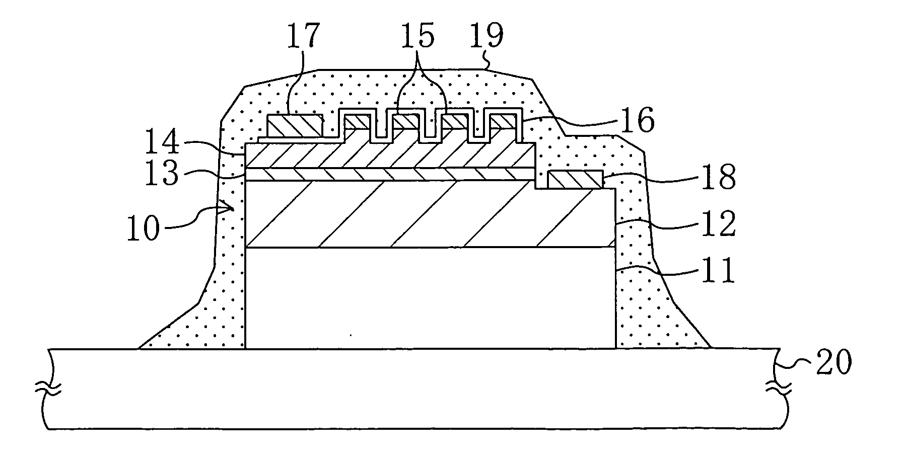
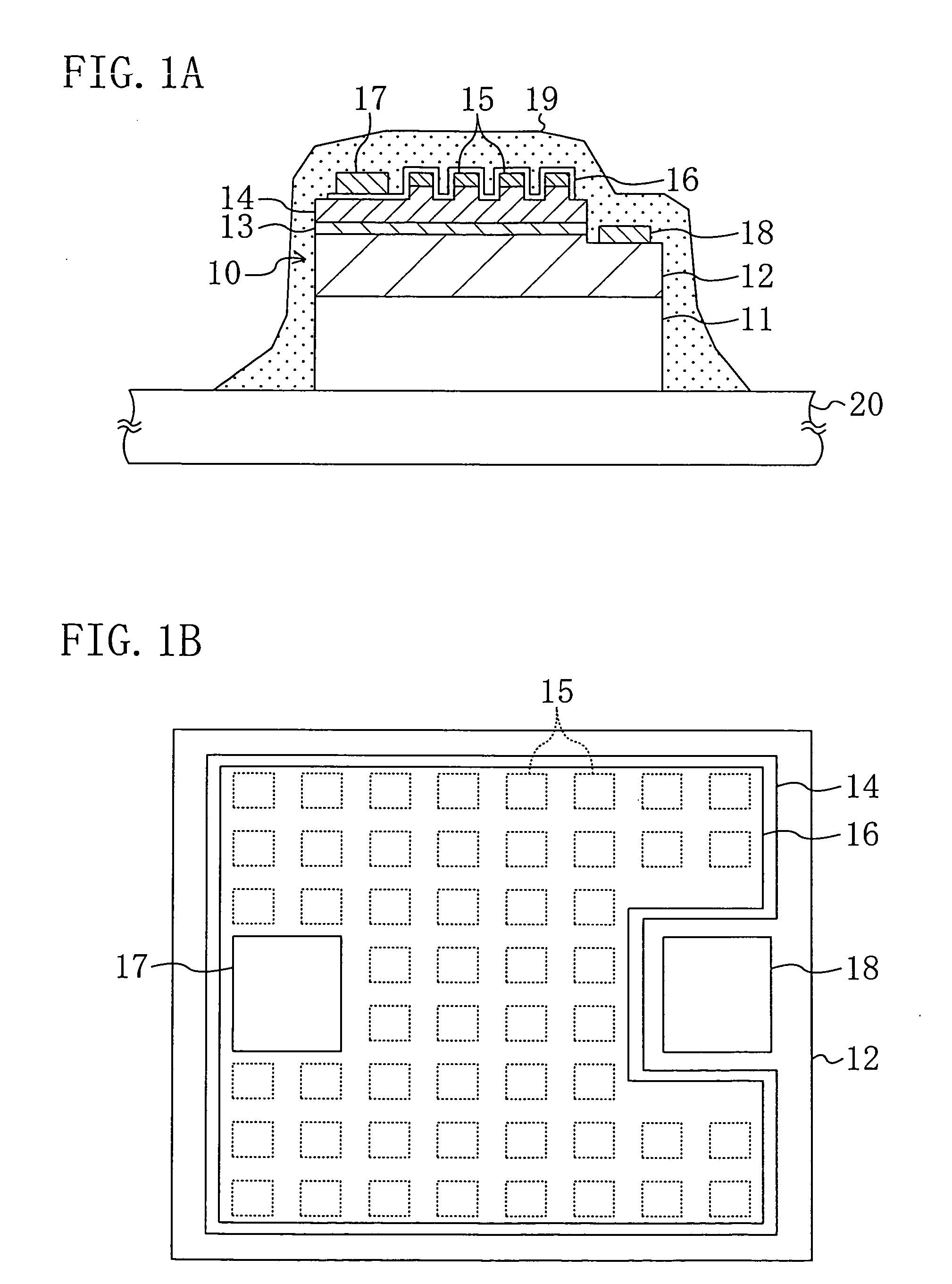
[0126]FIG. 1A shows a cross-sectional structure of a semiconductor light emitting device according to the first embodiment and FIG. 1B shows a plan structure thereof.

[0127] As shown in FIGS. 1A and 1B, a semiconductor light emitting device according to the first embodiment is composed of: a blue light emitting diode 10 mounted at a specified position on a package 20 as a mounting member; a red light emitting layer 15 grown epitaxially on the blue light emitting diode 10; and an insulating material 19 containing an yttrium aluminum garnet (YAG) fluorescent material. In FIG. 1B, the depiction of the insulating material 19 is omitted.

[0128] The blue light emitting diode 10 is composed of: an n-type semiconductor layer 12 made of n-type GaN; an active layer 13 having a multiple quantum well structure made of InGaN; and a p-type semiconductor layer 14 made of p-type Al0.05Ga0.95N which ...

embodiment 2

[0152] A second embodiment of the present invention will be described with reference to the drawings.

[0153]FIG. 5 shows a cross-sectional structure of a semiconductor light emitting device according to the second embodiment. The description of the components shown in FIG. 5 which are the same as those shown in FIG. 1A will be omitted by retaining the same reference numerals.

[0154] As shown in FIG. 5, the blue light emitting diode 10 in which the red light emitting layer 15 is formed selectively on the p-type semiconductor layer 14 is mounted by so-called flip-chip mounting such that the red light emitting layer 15 is opposed to the mounting surface of the package 20.

[0155] The p-type semiconductor layer 14 and the red light emitting layer 15 are connected electrically to the p-side electrode pad (not shown) of the package 20 by the p-side electrode 17 made of a multilayer film of platinum (Pt) and gold (Au) and a first bump 22 made of silver. On the other hand, the n-side electro...

embodiment 3

[0159] A third embodiment of the present invention will be described with reference to the drawings.

[0160]FIG. 6A shows a cross-sectional structure of a semiconductor light emitting device according to the third embodiment and FIG. 6B shows a plan structure thereof. The description of the components shown in FIGS. 6A and 6B which are the same as those shown in FIGS. 1A and 1B will be omitted by retaining the same reference numerals.

[0161] As shown in FIGS. 6A and 6B, the semiconductor light emitting device according to the third embodiment is composed of: the blue light emitting diode 10 mounted at a specified position on the package 20 as a mounting member; the red light emitting layer 15 grown epitaxially on the blue light emitting diode 10; and the insulating material 19 containing an yttrium aluminum garnet (YAG) fluorescent material.

[0162] The third embodiment is different from the first embodiment in that the transparent electrode 16 made of ITO covers only the upper surfac...


PUM


Abstract

A semiconductor light emitting device is composed of a blue light emitting diode, a red light emitting layer grown epitaxially on the blue light emitting diode, and an insulating material containing a YAG fluorescent material. The red light emitting layer is made of, e.g., undoped In0.4Ga0.6N having a forbidden band width of 1.9 eV and formed on a p-type semiconductor layer to have a configuration consisting of a plurality of mutually spaced-apart islands.

Description

CROSS-REFERENCE TO RELATED APPLICATIONS [0001] The teachings of Japanese Patent Applications JP 2004-42329 and JP 2004-42330, each filed Feb. 19, 2004, are entirely incorporated herein by reference, inclusive of the claims, specification, and drawings. BACKGROUND OF THE INVENTION [0002] The present invention relates to a semiconductor light emitting device which is applicable to, e.g., a white light emitting diode and to a method for fabricating the same. [0003] A gallium nitride-based (GaN-based) group III-V nitride semiconductor (InGaAlN) in which GaN has a large forbidden bandwidth of, e.g., 3.4 eV at a room temperature is a material which can implement a light emitting device capable of a high output in the blue or green wavelength band or even in the ultraviolet wavelength band. The GaN-based semiconductor has already been commercialized as a blue / green light emitting diode in various display panels, large-scale display devices, and traffic signals. [0004] On the other hand, a ...

Claims


Application Information

Patent Timeline
Patent Type & Authority Applications(United States)
IPC IPC(8): H01L29/20H01L33/06H01L33/32H01L33/42H01L33/50H01L33/56H01L33/62
CPCH01L33/08H01L24/03H01L24/05H01L24/16H01L2224/05001H01L2224/05017H01L2224/05023H01L2224/05111H01L2224/05124H01L2224/05144H01L2224/05155H01L2224/05169H01L2224/05558H01L2224/05568H01L2224/05644H01L2224/0603H01L2224/06102H01L2224/14H01L2224/1703H01L2924/00014
Inventor UEDA, TETSUZO
Owner PANASONIC CORP
Why Eureka
Try Eureka