Semiconductor device gate structure and method of forming the same

a gate structure and semiconductor technology, applied in the field of semiconductor devices, can solve the problems of damage to the single-crystalline layer, depletion of fully lean-channel structured mos transistors, and increase the junction capacitance between the source and drain regions, so as to prevent a short channel effect or narrow width effect

Inactive Publication Date: 2005-08-25
SAMSUNG ELECTRONICS CO LTD
View PDF14 Cites 72 Cited by
  • Summary
  • Abstract
  • Description
  • Claims
  • Application Information

AI Technical Summary

Benefits of technology

[0015] Embodiments of the invention provide a gate structure of a semiconductor d

Problems solved by technology

However, the fin-structured MOS transistor is disadvantageous in that because a plurality of channel fins is arranged in parallel along a width direction of the gate, thus the channel region and the source/drain regions are enlarged in the MOS transistor.
In addition, the fin-structured MOS transistor also has also problem that a junction capacitance between the source and drain regions is increased as the channel number is increased.
However, the fully depleted lean-channel structured MOS tra

Method used


Image

  • Semiconductor device gate structure and method of forming the same
  • Semiconductor device gate structure and method of forming the same
  • Semiconductor device gate structure and method of forming the same

Examples


Embodiment Construction

[0039] The present invention now will be described more fully hereinafter with reference to the accompanying drawings in which exemplary embodiments of the present invention are shown.

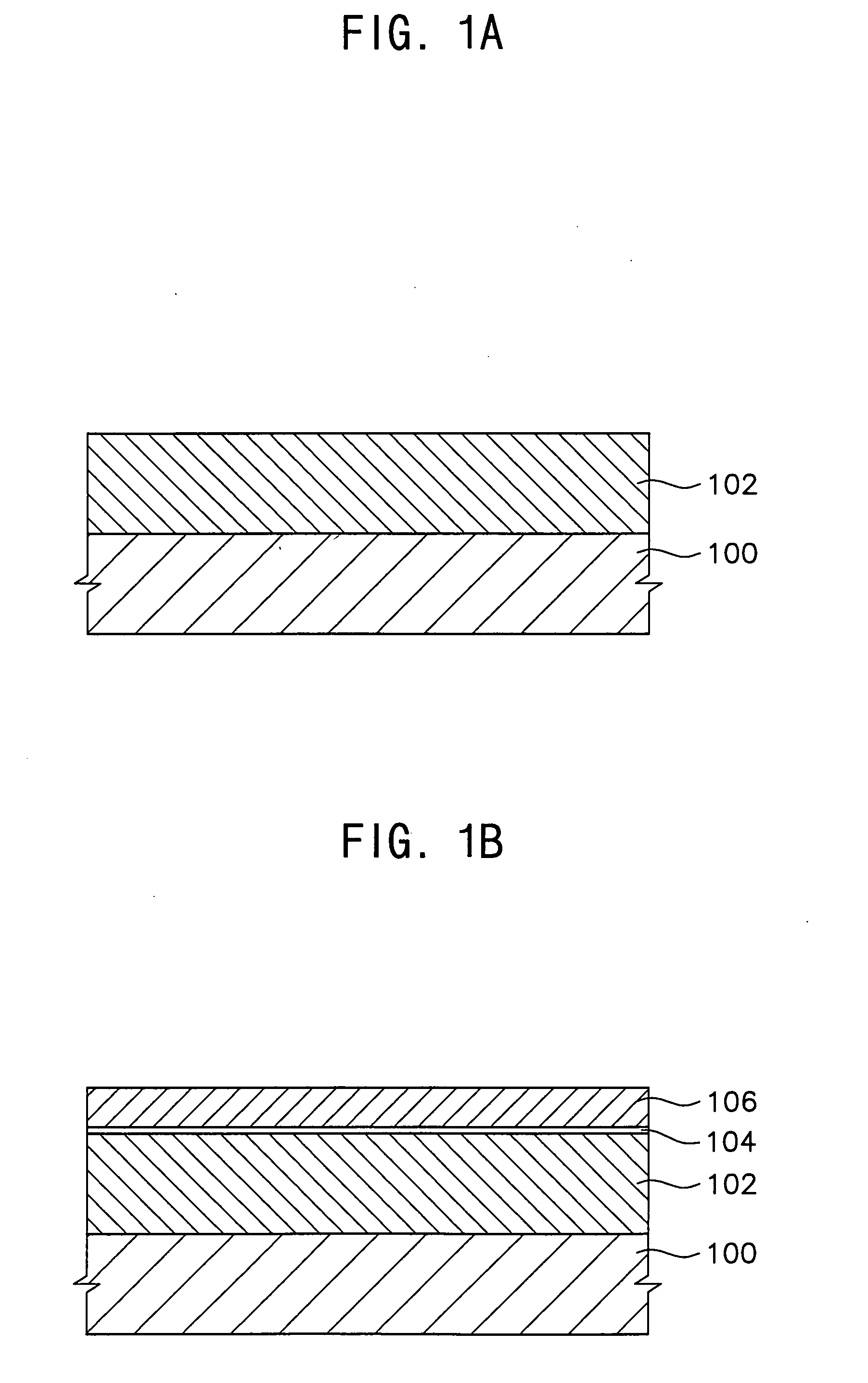
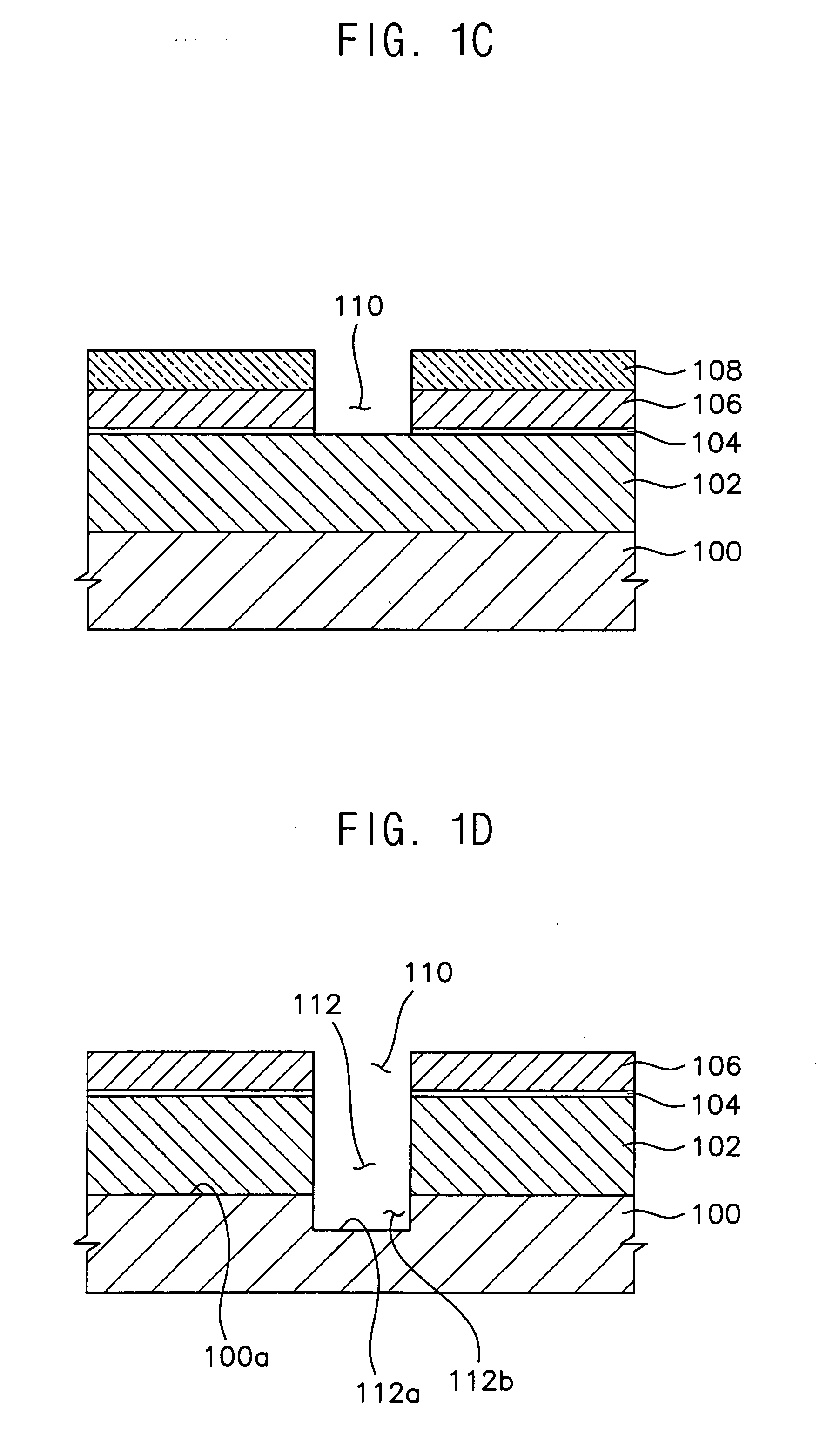
[0040]FIGS. 1A to 1I are cross sectional views illustrating processing steps of forming a gate structure according to an embodiment of the present invention, and FIG. 2 is a perspective view of the gate structure in accordance with FIGS. 1A to 1I.

[0041] Referring to FIG. 1A, a sacrificial layer 102 is formed on a semiconductor substrate 100 such as a silicon wafer. The sacrificial layer 102 exemplarily comprises silicon germanium, and is formed by a chemical vaporization deposition (CVD) process or an epitaxial growth process. In particular, an ultra high vacuum CVD (UVCVD) process or a low pressure CVD (LPCVD) is usually used for forming the sacrificial layer 102 using a silicon source gas such as silane gas (SiH4), a germanium source gas such as germanium hydride (GeH4), and a carrier gas such as h...


PUM


Abstract

A MOS transistor includes a gate structure extending forrom a semiconductor substrate in a vertical direction is disclosed. The gate structure includes a gate electrode extending from the substrate in a vertical direction, and a gate insulation layer enclosing the gate electrode. A channel pattern encloses the gate insulation layer, and a first conductive pattern extends from a lower portion of the channel pattern in a first direction verticalperpendicular to the channel pattern and in parallel with the substrate. A second conductive pattern extends from an upper portion of the channel pattern in a second direction verticalperpendicular to the channel pattern and in parallel with the substrate. Accordingly, the channel length of the MOS transistor is determined by a distance between the first and second conductive patterns, and a channel width of the MOS transistor is determined by a diameter of the gate structure. Short channel and narrow width effects are sufficiently prevented in a MOS transistor.

Description

CROSS-REFERENCE TO RELATED APPLICATIONS [0001] This application relies for priority upon Korean Patent Application No. 2004-10882 filed on Feb. 19, 2004, the content of which is herein incorporated by reference in its entirety. BACKGROUND OF THE INVENTION [0002] 1. Field of the Invention [0003] This disclosure relates to a semiconductor device and a method of manufacturing the same. More particularly, disclosure relates to a gate structure and a metal oxide semiconductor (MOS) transistor having the gate structure and a method of forming the gate structure and the MOS transistor. [0004] 2. Description of the Related Art [0005] As semiconductor devices become more highly integrated, active regions, in where various conductive structures are positioned become reduced in a size and a channel length ofin the a MOS transistor in the active region is also shortened. When the channel length is decreased, a source or a drain of the MOS transistor has much more an increased effect on an elect...

Claims


Application Information

Patent Timeline
IPC IPC(8): H01L21/28H01L21/316H01L21/336H01L21/8234H01L21/84H01L27/12H01L29/423H01L29/49H01L29/78H01L29/786
CPCH01L21/823487H01L29/42384H01L29/4908H01L29/78642H01L29/66742H01L29/78618H01L29/66666B26D1/18B26D7/01
Inventor YOUN, JAE-MANPARK, DONG-GUNLEE, CHOONG-HOYOSHIDA, MAKOTOLEE, CHUL
Owner SAMSUNG ELECTRONICS CO LTD
Why Eureka
Try Eureka