Liquid crystal displays using organic insulating material and manufacturing methods thereof

a liquid crystal display and organic insulating material technology, applied in non-linear optics, instruments, optics, etc., can solve the problems of difficult to make a uniform cell gap, difficult to shield light leakage perfectly, and non-uniform thickness of liquid crystal layer, etc., to achieve the effect of reducing the coupling capacitan

Inactive Publication Date: 2005-08-25
SAMSUNG DISPLAY CO LTD
View PDF39 Cites 23 Cited by
  • Summary
  • Abstract
  • Description
  • Claims
  • Application Information

AI Technical Summary

Benefits of technology

[0010] It is therefore an object of the present invention to allow a reduction in the coupling capacitance generated between a data line and a pixel electrode.

Problems solved by technology

However, misalignment between the TFT substrate and the color filter substrate may make it hard to shield the light leakage perfectly.
Since the black matrix 11 is formed on the TFT, the height difference between the portions near the TFT and the pixel electrode 12 can become larger to make defects of the alignment layer, thereby causing leakage.
Because of the height difference in the color filter substrate and in the TFT substrate, it may be difficult to make a uniform cell gap.
Therefore, the thickness of the liquid crystal layer becomes non-uniform, and display characteristics become worse.
Moreover, the spacers on the pixel electrode 12 may cause a defect in the alignment layer and may cause the light from the backlight unit to be scattered, thereby causing the low transmittance of the liquid crystal cell and the light leakage.

Method used


Image

  • Liquid crystal displays using organic insulating material and manufacturing methods thereof
  • Liquid crystal displays using organic insulating material and manufacturing methods thereof
  • Liquid crystal displays using organic insulating material and manufacturing methods thereof

Examples


first embodiment

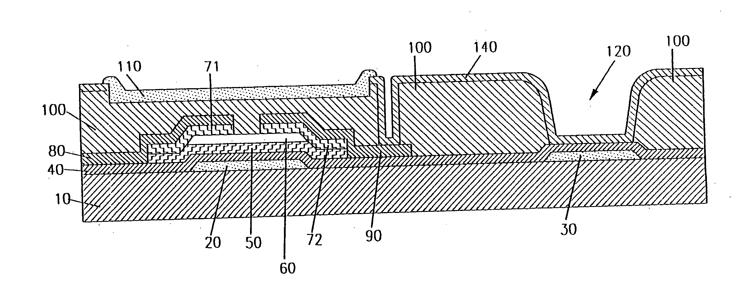
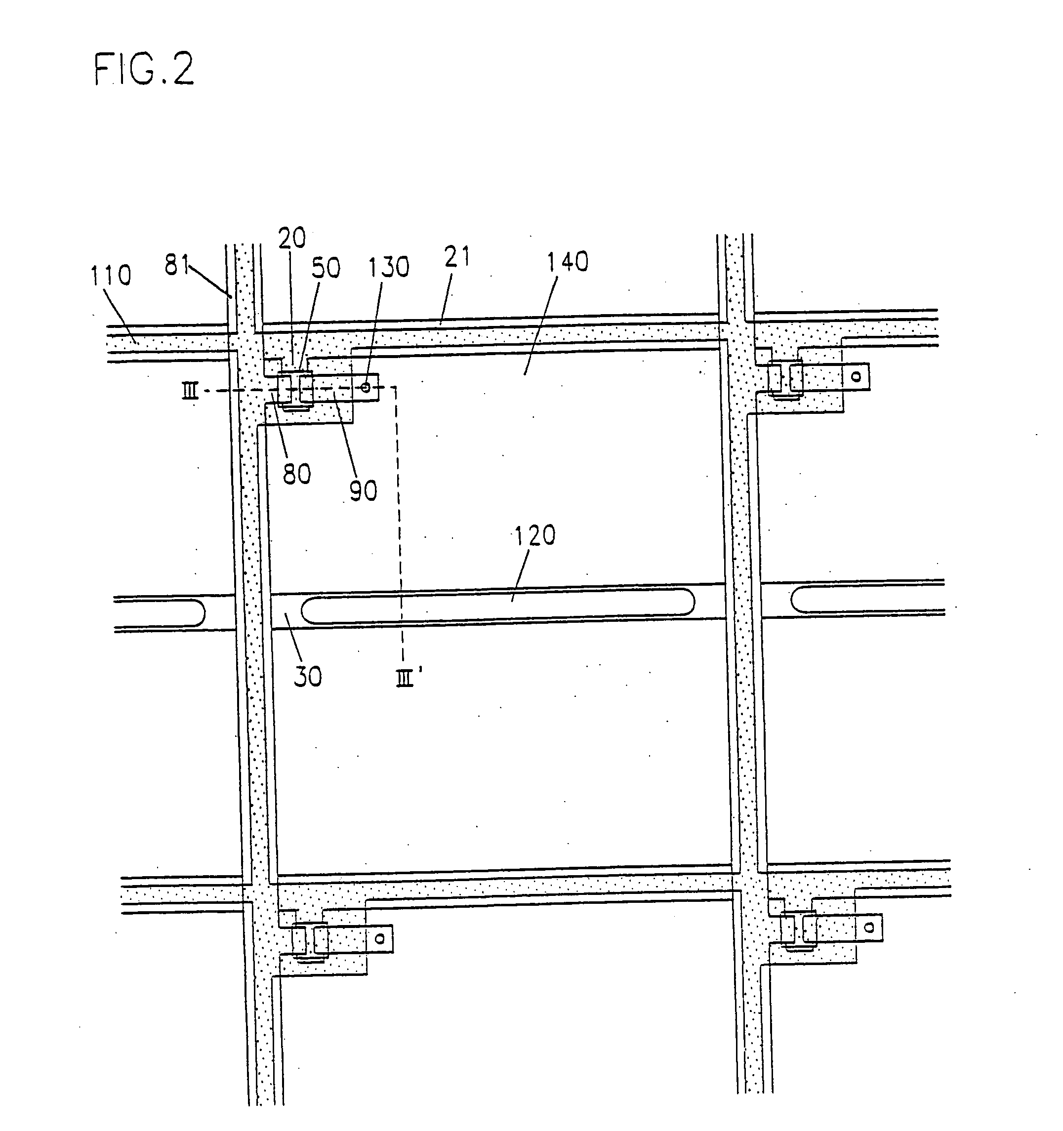
[0041]FIG. 2 shows a layout of a TFT substrate according to the present invention, and FIG. 3 illustrates a cross-sectional view of a TFT substrate shown in FIG. 2 along the line III-III′.

[0042] As shown in FIGS. 2 and 3, a gate line 21 which transmits scanning signals from the outside, a gate electrode 20 which is a branch of the gate line 21 and a storage capacitor electrode 30 which is parallel to the gate line 21 are formed on a transparent insulating substrate 10 such as glass. A gate insulating layer 40 is formed thereon.

[0043] A data line 81 which is perpendicular to the gate line 21 and transmits display signals from the outside is formed on the portion of gate insulating layer 40. An amorphous silicon (a-Si) layer 50 is formed on the gate insulating layer 40 on the gate electrode 20. An etch stopper layer 60 and an ohmic contact layer 71 and 72 made of heavily doped amorphous silicon with n type ions (n+ a-Si) are formed on the a-Si layer 50 in sequence. A source electrode...

second embodiment

[0053] According to the present invention, as shown in FIG. 4, the portion of the passivation layer 100 on the storage capacitor electrode 30 is removed, and the portion of the gate insulating layer 40 on the storage capacitor electrode 30 is thinner than the other portions. To keep the uniform thickness of the portion of the gate insulating layer 40 on the storage capacitor electrode 30, the gate insulating layer 40 may include two layers which have different etch rates, and the portion of the upper layer on the storage capacitor electrode 30 may be removed.

third embodiment

[0054] According to the present invention, as illustrated in FIG. 5, a metal pattern 31 is formed on the portion of the gate insulating layer 40 on the storage capacitor electrode 30. The metal pattern 31 is connected to the storage capacitor electrode 30 through a contact hole 32 in the gate insulating layer 40, and covered with the passivation layer 100.


PUM

PropertyMeasurementUnit
dielectric constantaaaaaaaaaa
optical densityaaaaaaaaaa
resistanceaaaaaaaaaa

Abstract

A passivation layer is formed by coating a flowable insulating material on the substrate where a thin film transistor and a storage capacitor electrode, and a pixel electrode is formed on the passivation layer. A portion of the passivation layer is etched using the pixel electrode as a mask to make a groove on the thin film transistor, and then a black matrix is formed by filling an organic black photoresist in the groove. To increase the storage capacitance, a portion of the passivation layer is removed or to form a metal pattern on the storage capacitor electrode. A flowable insulating material is used as a gate insulating layer to planarize the substrate. In the case of the etch stopper type thin film transistor, a photo definable material is used as the etch stopper layer to reduce the parasitic capacitance between the gate electrode and the drain electrode.

Description

BACKGROUND OF THE INVENTION [0001] (a) Field of the Invention [0002] The present invention relates to a thin film transistor liquid crystal display, more specifically to a thin film transistor liquid crystal display whose black matrix is formed on a thin film transistor substrate. [0003] (b) Description of the Related Art [0004] Most liquid crystal displays include a thin film transistor (TFT) substrate and a color filter substrate. Black matrix is generally formed on the color filter substrate and is used to shield the light leakage in the portions between pixels. However, misalignment between the TFT substrate and the color filter substrate may make it hard to shield the light leakage perfectly. For that reason, a method of forming the black matrix on TFTs, which is called black matrix on TFT (BM on TFT), was recently suggested. [0005]FIG. 1 illustrates a cross-sectional view of a conventional BM on TFT type TFT substrate. [0006] As shown in FIG. 1, a gate electrode 2 and a storag...

Claims


Application Information

Patent Timeline
Patent Type & Authority Applications(United States)
IPC IPC(8): G02F1/1333G02F1/1362
CPCG02F1/136209G02F2001/133357G02F1/136227G02F1/136213G02F1/133357
Inventor RHO, SOO-GUYLEE, JUNG-HO
Owner SAMSUNG DISPLAY CO LTD
Why Eureka
Try Eureka