Drill hole inspection method for printed circuit board fabrication

a technology for printing circuit boards and inspection methods, which is applied in the direction of circuit inspection/indentification, printed element electric connection formation, instruments, etc., and can solve problems such as failure of the fabrication process, shrinkage of artwork, and defects in the pcb or pcb artwork

Inactive Publication Date: 2005-09-01
MANIA BARCO
View PDF4 Cites 26 Cited by
  • Summary
  • Abstract
  • Description
  • Claims
  • Application Information

AI Technical Summary

Benefits of technology

[0009] The present invention is directed to the inspection of PCB holes to determine if the holes have or have not been placed within an acceptable area of a pad on the surface of a PCB. Specifically, it is preferred that a PCB hole, e.g., a plated through-hole or a hole otherwise used for electrical connection is placed with at least some predetermined amount of pad material surrounding the hole. The method and apparatus of the present invention solve the problems of the prior art by including a more robust method to process hole images.

Problems solved by technology

However carefully the PCBs are produced, defects may be present in the PCB or in the PCB artwork which would render the printed circuit board useless.
These defects can have a variety of causes, including shrinkage in the artwork or failures in the fabrication process.
A Golden Board System does not detect errors in subsequent boards that were also in the golden board.
Should the shrinkage exceed a certain value, the board is considered by these systems to be defective.
Should this condition not be met, an error signal may be generated.
A substrate itself may be distorted or the artwork employed may have been produced out of calibration.
It is entirely conceivable that slight distortions could result in for example, an end substrate on the panel or / and circuit on the substrate being mis-registered by one or more pixels.
Another cause of imperfections is the misalignment of various processing steps.
The detection of misaligned holes on pads is particularly difficult to determine, as it requires the detection of both the hole and pad edge, and is thus particularly difficult to accurately determine.
If the area determined from the image exceeds the error threshold, then the hole is rejected as being unacceptable.

Method used


Image

  • Drill hole inspection method for printed circuit board fabrication
  • Drill hole inspection method for printed circuit board fabrication
  • Drill hole inspection method for printed circuit board fabrication

Examples


Embodiment Construction

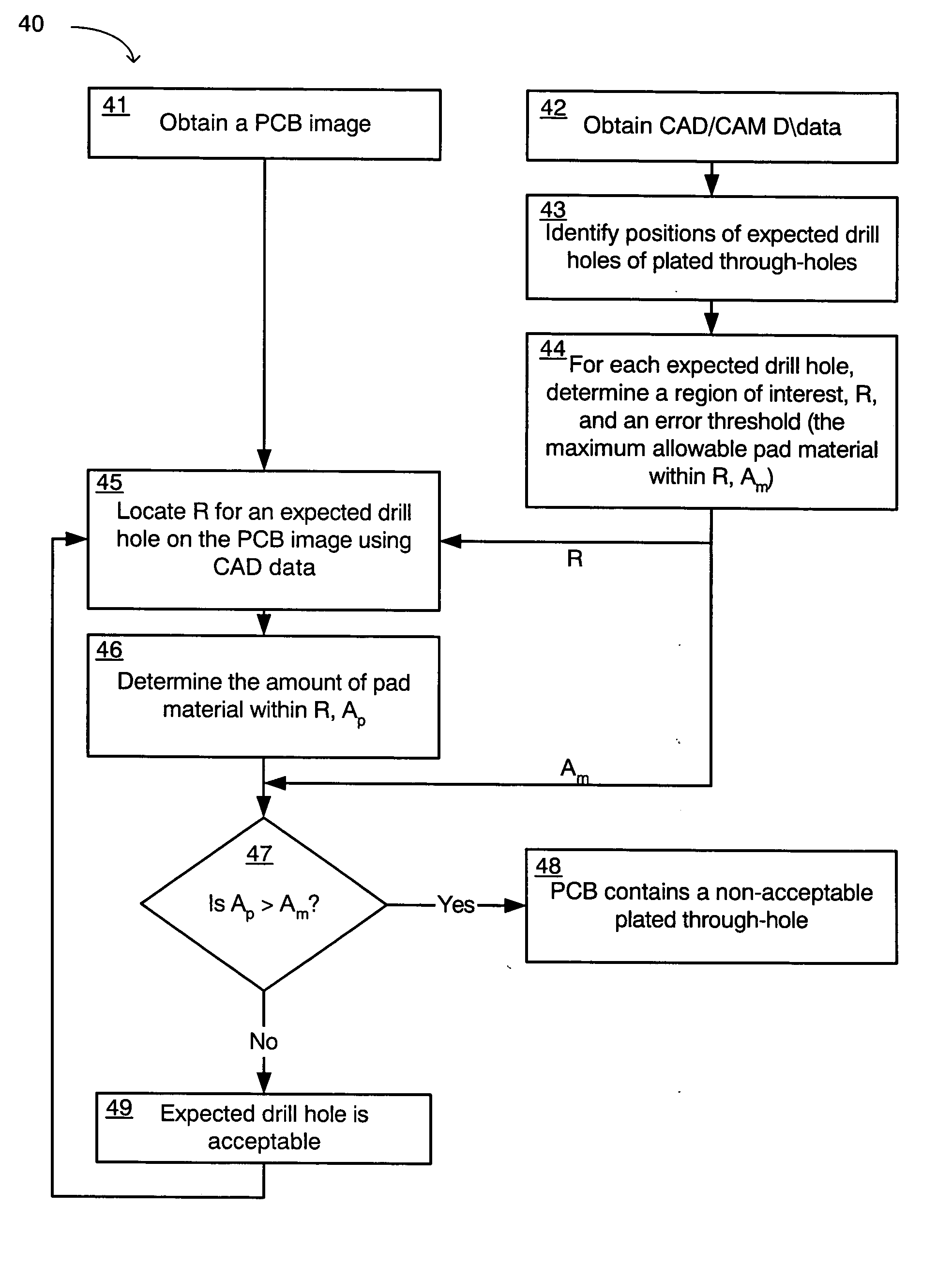
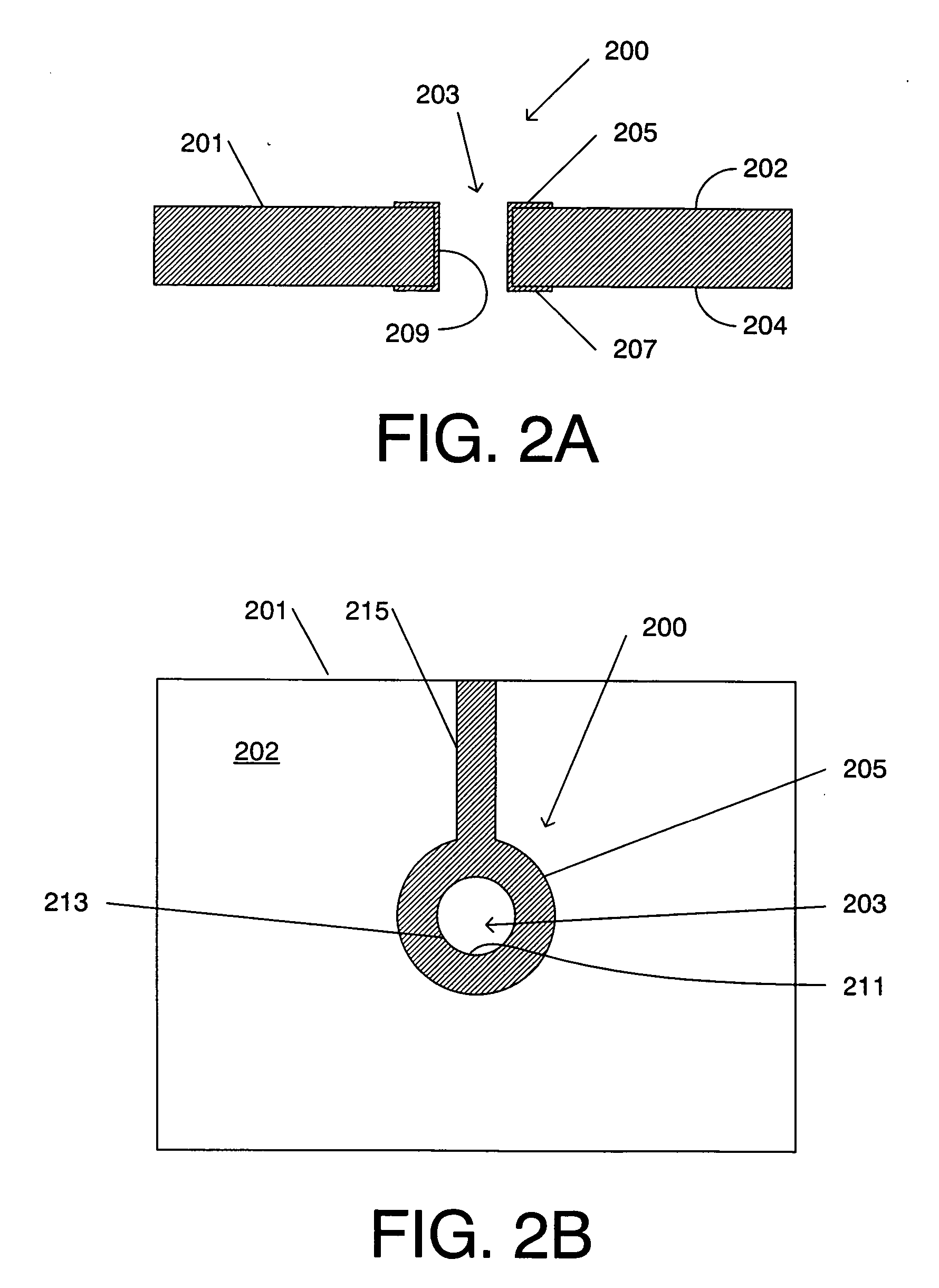
[0028] Presented herein are an optical inspection method and an apparatus. The optical inspection method and apparatus of the present invention is particularly useful for the inspection of holes in printed circuit boards. In particular, the holes referred to herein are placed through a conducting pad on the surface of a PCB for attachment to electrical components. The conducting pad provides an electrical conduit to other locations on the PCB surface, or to other circuit board sides, for example as a plated through-hole used for a two-sided part or a multi-layer board. The hole provides mechanical support or electrical contacts for electrical components that are mounted to the hole.

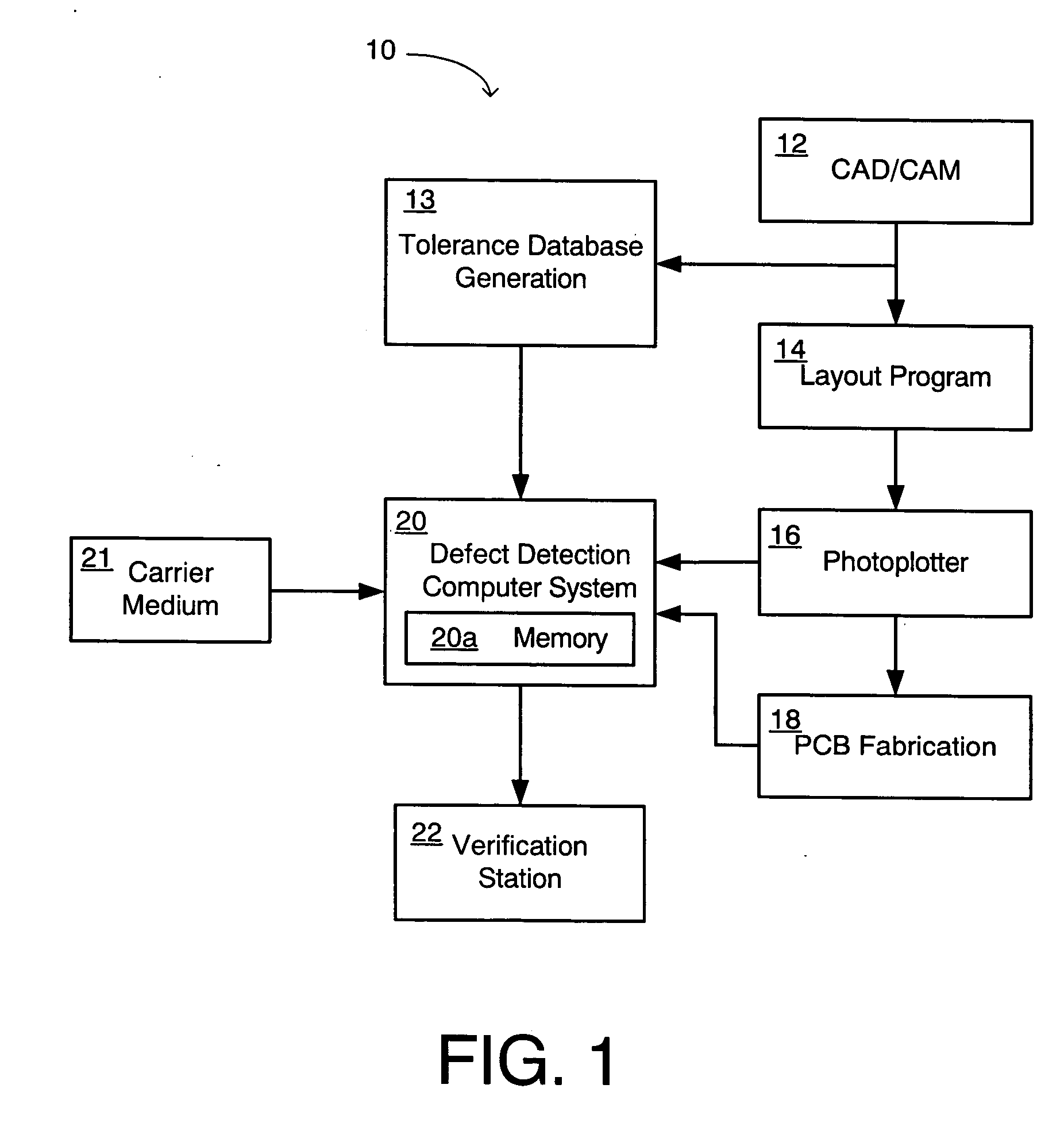
[0029]FIG. 1 shows a simplified schematic of a series of devices representative of an overall system 10 used in the fabrication of a PCB. Typically, the circuits to be fabricated on the PCB are generated using a computer aided design / computer aided manufacturing (CAD / CAM) apparatus 12 which generates a d...


PUM


Abstract

The automated inspection of features on printed circuit boards is compatible with automated manufacturing technology and greatly speeds the production of useful boards. One printed circuit board feature that can be difficult to inspect is the placement of holes surrounded by pad material. The present invention provides a more robust method and apparatus for inspecting holes to determine if they are surrounded by a pad material. Hole Images are processed to highlight the hole and adjacent pad material. Automated design and manufacturing data is combined with an indication of what forms an acceptable hole based on surface area measurement of pad material on the printed circuit board. The method and apparatus then compares measured areas with a calculated error threshold to determine if the hole is placed within an acceptable region of the printed circuit board. The invention also includes computer readable media containing programs to execute the methods of the invention

Description

BACKGROUND OF THE INVENTION [0001] This invention relates to systems for inspecting printed circuit boards (PCB), and more specifically to systems and methods for determining the integrity of drill pads of printed circuit boards. BACKGROUND [0002] Printed circuit boards are today manufactured by a process that is almost completely automated. The circuits for a particular printed circuit board are generated using a computer aided design (CAD) machine which generates a schematic of the PCB and also provides the board layout for all of the devices thereon. The PCB layout information is provided to a device such as a laser plotter that exposes the artwork needed to fabricate the PCB. The artwork comprises a series of transparent and opaque areas as features corresponding to the PCB devices. The PCB layout information is also provided to equipment for forming other PCB elements, such as drill presses and plating equipment that provides holes for mounting through-hole components. These da...

Claims


Application Information

Patent Timeline
Patent Type & Authority Applications(United States)
IPC IPC(8): G01R31/28G06K9/00G06T7/00H05K1/02H05K1/11H05K3/00H05K3/42
CPCG01R31/2813G06T7/0004H05K1/0269H05K2203/163H05K3/0047H05K3/42H05K1/116
Inventor KOHLER, JAMES P.WELTI, GENE D.
Owner MANIA BARCO
Why Eureka
Try Eureka