Method for manufacturing semiconductor device

a manufacturing method and semiconductor technology, applied in semiconductor devices, semiconductor/solid-state device details, electrical apparatus, etc., can solve the problems of forming a lot the speed of semiconductor devices is significantly increased, and the problem of a large number of micro pores in the insulating film is not easy to achieve. , to achieve the effect of excellent electrical properties and reliability

Inactive Publication Date: 2005-09-01
SANYO ELECTRIC CO LTD
View PDF11 Cites 51 Cited by
  • Summary
  • Abstract
  • Description
  • Claims
  • Application Information

AI Technical Summary

Benefits of technology

[0013] Therefore, the object of the present invention is to solve the above-described problems. Specifically, the object of the present invention is to provide a method for manufacturing a semiconductor device having excellent electrical properties and reliability by using a porous insulating film.

Problems solved by technology

In recent years, the speed of semiconductor device has significantly increased, and concurrently, transmission delay due to the lowered signal transmission speed caused by wiring resistance in a multilayer wiring portion, and parasitic capacitance between wirings or between wiring layers has caused problems.
Such problems tend to be more significant, because wiring resistance rises and parasitic capacitance increases with the reduction of wiring width and wiring distance accompanying the high integration of semiconductor devices.
This results in formation of a lot of micro pores in the insulating film.
However, there has been a problem that heat treatment at such a high temperature causes the reliability of copper wirings to lower.
In the steps of dry etching and ashing in the Damascene method, the porous low-k film is easily undergone charging damage by plasma.
There has also been a problem that the properties of the porous low-k film as an interlayer insulating film are thereby affected to lower the electrical properties and reliability of the semiconductor device.

Method used


Image

  • Method for manufacturing semiconductor device
  • Method for manufacturing semiconductor device
  • Method for manufacturing semiconductor device

Examples


Embodiment Construction

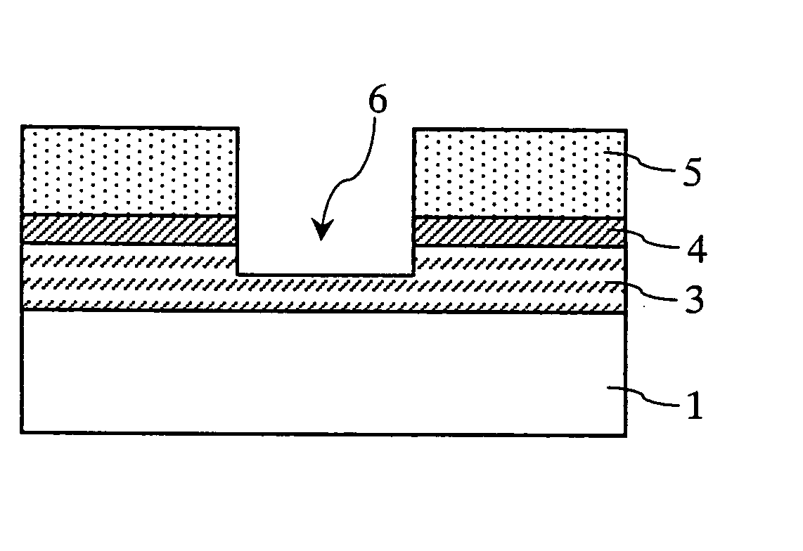
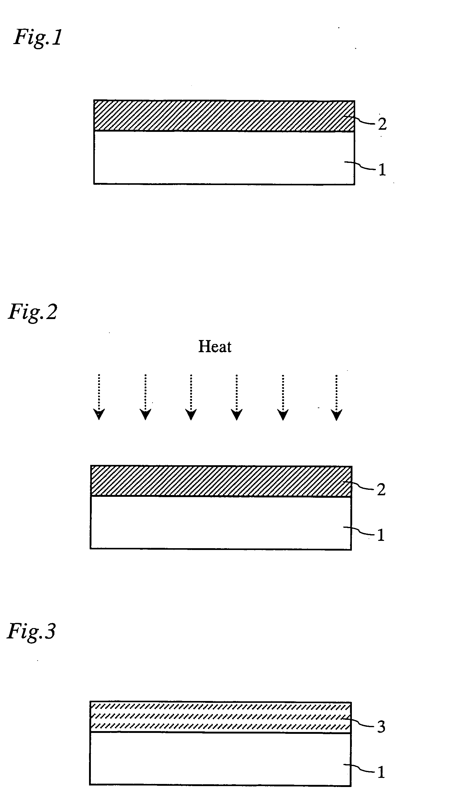
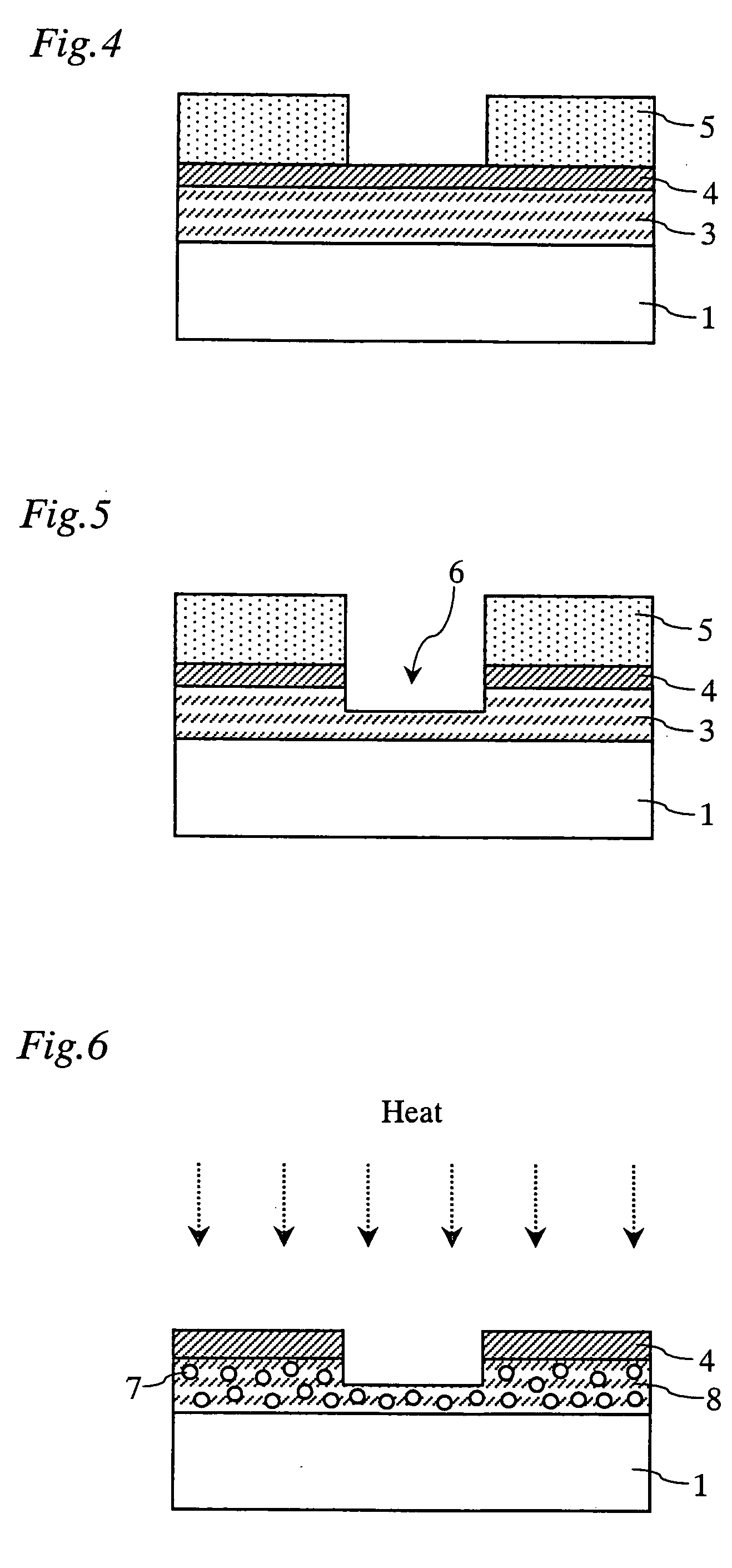
[0034] The present inventor conducted repetitive studies, and found that a semiconductor device that excelled in electrical properties and reliability could be manufactured by forming a wiring trench in the stage of curing polysiloxane, and thereafter performing heat treatment at a high temperature to vaporize and remove a pore-generating material. According to this method, the wiring trench is formed in the state wherein no pores are present in the interlayer insulating film. Therefore, during dry etching and ashing, the interlayer insulating film is not damaged by plasma charging, and the cleaning solution does not permeate into the interlayer insulating film. Furthermore, since pores are formed by decomposing and vaporizing the pore-generating material after the formation of the wiring trench, the relative dielectric constant of the interlayer insulating film can be lowered. Therefore, a semiconductor device having a small parasitic capacitance between wiring layers, excellent el...


PUM

PropertyMeasurementUnit
temperatureaaaaaaaaaa
dielectric constantaaaaaaaaaa
temperatureaaaaaaaaaa

Abstract

A heat treatment is performed to an insulating film composition, formed on a semiconductor substrates at a temperature of 350° C. in an inert gas ambient to form a non-porous insulating film. Next, dry etching is performed using a resist pattern as a mask to form a trench in the non-porous insulating film, ashing is performed to remove the resist pattern, and the surface of the semiconductor substrate is cleaned. Thereafter, a second heat treatment is performed for the non-porous insulating film to form a porous insulating film. Since the second heat treatment is performed in an oxidizing-gas atmosphere, the pore-generating material can be removed at a temperature lower than the temperature of conventional methods to form an insulating film having a low dielectric constant.

Description

BACKGROUND OF THE INVENTION [0001] 1. Field of the Invention [0002] The present invention relates to a method for manufacturing a semiconductor device, and more specifically to a method for manufacturing a semiconductor device using a porous low dielectric constant insulating film. [0003] 2. Background Art [0004] In recent years, the speed of semiconductor device has significantly increased, and concurrently, transmission delay due to the lowered signal transmission speed caused by wiring resistance in a multilayer wiring portion, and parasitic capacitance between wirings or between wiring layers has caused problems. Such problems tend to be more significant, because wiring resistance rises and parasitic capacitance increases with the reduction of wiring width and wiring distance accompanying the high integration of semiconductor devices. [0005] Heretofore, in order to prevent signal delay caused by such a rise of wiring resistance and increase of parasitic capacitance, a copper wir...

Claims


Application Information

Patent Timeline
Patent Type & Authority Applications(United States)
IPC IPC(8): H01L21/00H01L21/02H01L21/3205H01L21/311H01L21/314H01L21/316H01L21/4763H01L21/768H01L23/52
CPCH01L21/02063H01L21/02107H01L21/02203H01L21/02282H01L21/02337H01L21/76841H01L21/31116H01L21/31138H01L21/31695H01L21/7682H01L21/02362H01L2221/1047
Inventor MISAWA, KAORIOHASHI, NAOFUMI
Owner SANYO ELECTRIC CO LTD
Why Eureka
Try Eureka