Resin-encapsulated semiconductor device and lead frame, and method for manufacturing the same

a resin-encapsulated semiconductor and lead frame technology, applied in semiconductor devices, solid-state devices, basic electric elements, etc., can solve the problems of difficult packaging and further miniaturization of resin-encapsulated semiconductor devices

Active Publication Date: 2005-09-08
III HLDG 12 LLC
View PDF8 Cites 108 Cited by
  • Summary
  • Abstract
  • Description
  • Claims
  • Application Information

AI Technical Summary

Benefits of technology

[0012] An object of the present invention is to provide a resin-encapsulated semiconductor device in which a plurality of semiconductor elements or coils and resistors for s

Problems solved by technology

However, due to limitations on the processing of a line and space (design of a wiring pattern) of a substrate to be mounted and limitations imposed by a method of mounting by a reflow process using a solder cream, the smallest possible pitch of the external terminals that allows these semiconductor devices to be

Method used


Image

  • Resin-encapsulated semiconductor device and lead frame, and method for manufacturing the same
  • Resin-encapsulated semiconductor device and lead frame, and method for manufacturing the same
  • Resin-encapsulated semiconductor device and lead frame, and method for manufacturing the same

Examples


embodiment 1

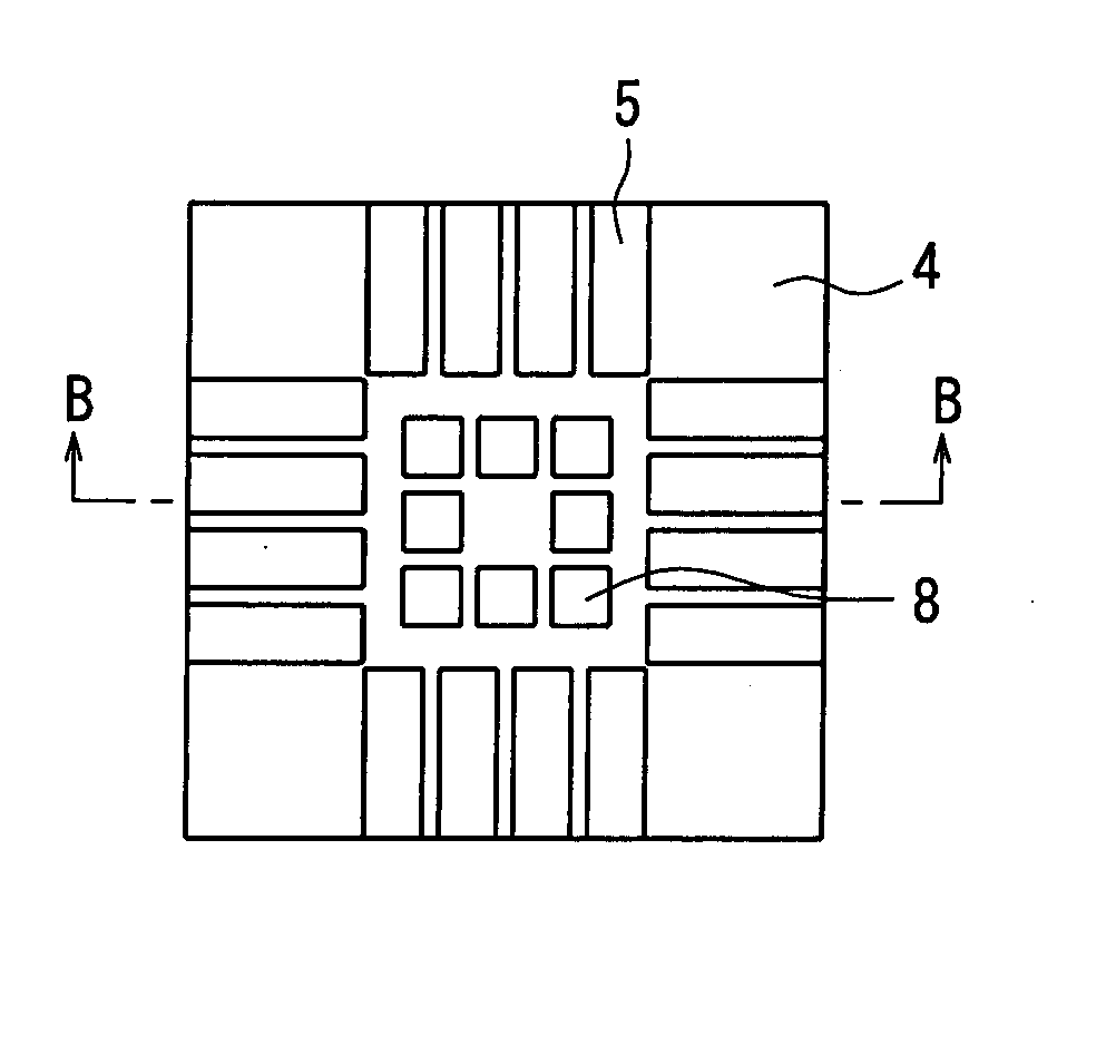
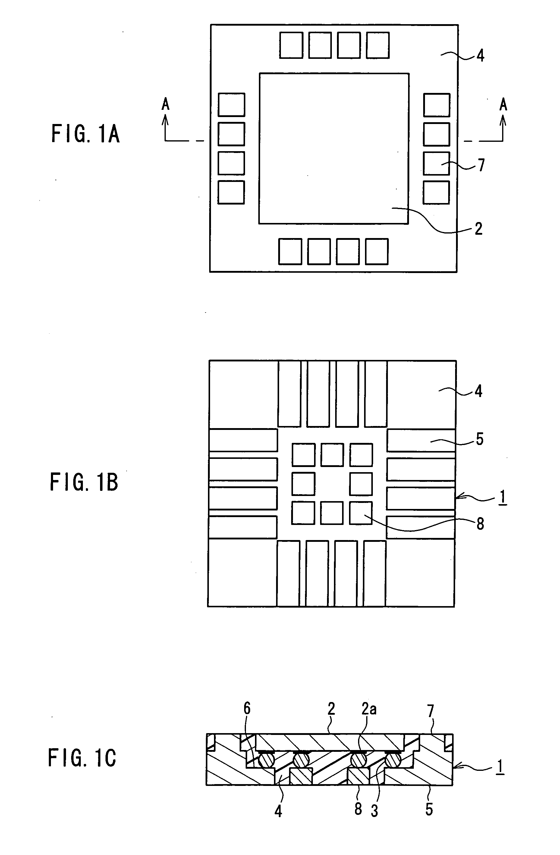
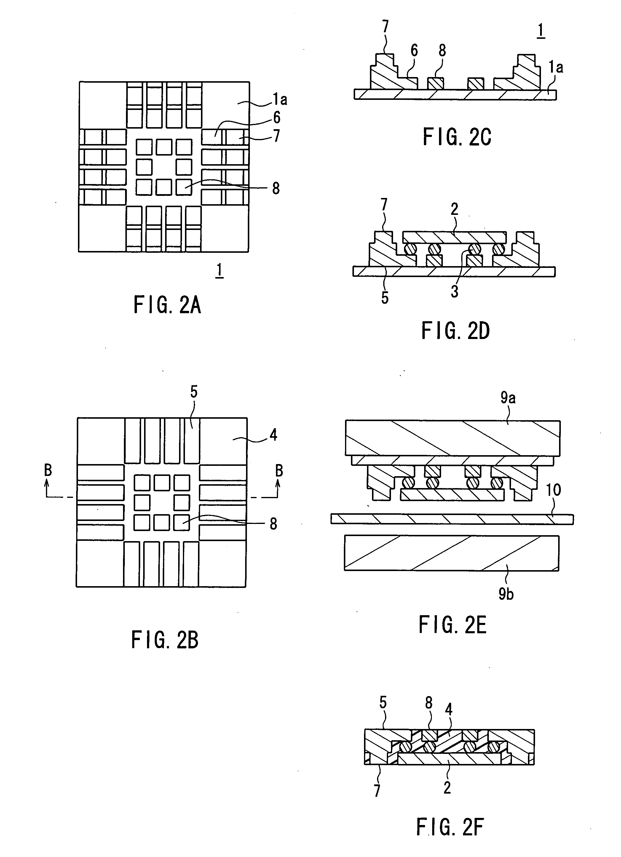
[0043]FIG. 1A is a plan view illustrating a resin-encapsulated semiconductor device according to Embodiment 1, FIG. 1B is a back view thereof, and FIG. 1C is a cross-sectional view thereof taken along line A-A in FIG. 1A.

[0044] As shown in FIG. 1C, the resin-encapsulated semiconductor device has s structure in which a first semiconductor element 2 is mounted on an upper surface of a lead frame 1 via metal bumps 3 by flip-chip bonding and a connection part located between the lead frame 1 and the first semiconductor element 2 is encapsulated with an encapsulating resin 4.

[0045] The lead frame 1 includes a plurality of first external terminal portions 5 arranged on a plane as shown in FIG. 1B and inner lead portions 6 formed of surfaces opposite to the first external terminal portions 5. Further, as shown in FIGS. 1A and 1C, second external terminal portions 7 are formed of uppermost surfaces of convex portions positioned in a part of the respective inner lead portions 6. The inner ...

embodiment 2

[0068]FIG. 7A is a plan view illustrating a resin-encapsulated semiconductor device according to Embodiment 2, FIG. 7B is a back view thereof, and FIG. 7C is a cross-sectional view thereof taken along line D-D in FIG. 7A. FIGS. 8A to 8G illustrate a manufacturing process of the resin-encapsulated semiconductor device shown in FIGS. 7A to 7C.

[0069] In this embodiment, as shown in FIG. 7C, second external terminal portions 28 of a lead frame 27 have a slightly different shape from that shown in the above embodiment, that is, have larger areas, on which solder balls 29 are provided. Further, in this embodiment, an encapsulating resin 30 is provided by potting as shown in FIG. 8E, although injection molding is conducted in the case shown in FIG. 2E. Furthermore, as shown in FIGS. 9A and 9B, a step of grinding the resin is carried out.

[0070]FIG. 8A is a plan view of the lead frame 27. FIG. 8B is a plan view of the resin-encapsulated semiconductor device manufactured by the process. FIG...

embodiment 3

[0077]FIG. 11A is a plan view illustrating a resin-encapsulated semiconductor device according to Embodiment 3, FIG. 11B is a back view thereof, and FIG. 11C is a cross-sectional view thereof taken along line F-F in FIG. 1A. The resin-encapsulated semiconductor device basically has the same structure as that shown in FIGS. 1A to 1C. In the resin-encapsulated semiconductor device of this embodiment, a resin 37 with a high dielectric constant is sandwiched between two terminals 36 provided in a region inside inner lead portions 6.

[0078] This configuration allows a formation of a resistor. In general, a resistor (square shape) is formed by printing and baking a thick film paste on an aluminum ceramic substrate. As the thick film paste to become a resistor, a ruthenium-oxide(RuO2)-based paste is used. Such a ruthenium-oxide(RuO2-based paste also can be used as the resin 37 with a high dielectric constant of this embodiment, and it is injected between the two terminals by a dispenser sy...


PUM


Abstract

There are provided a lead frame including a plurality of first external terminal portions 5 provided on a plane, inner lead portions 6 formed of back surfaces of the respective first external terminal portions and arranged so as to surround a region inside the inner lead portions, and second external terminal portions 7 formed of uppermost surfaces of convex portions positioned outside the respective inner lead portions; a semiconductor element 2 flip-chip bonded to the inner lead portions via bumps 3; and an encapsulating resin 4 encapsulating surroundings of the semiconductor element and the inner lead portions. The first external terminal portions are arranged in a lower surface region of the encapsulating resin along a periphery of the region, and the second external terminal portions are exposed on an upper surface of the encapsulating resin. A plurality of terminals 8 for electrical connection are provided in a grid pattern in a region inside the first external terminal portions and exposed on a lower surface of the encapsulating resin. A plurality of semiconductor elements or coils and resistors can be incorporated, and further semiconductor devices can be stacked.

Description

BACKGROUND OF THE INVENTION [0001] 1. Field of the Invention [0002] The present invention relates to a resin-encapsulated semiconductor device in which a semiconductor element is bonded on inner leads of a lead frame and the surroundings thereof are encapsulated with a resin, and that allows other semiconductor devices or functional components such as a resistor to be stacked in a vertical direction. [0003] 2. Description of the Related Art [0004] In recent years, in order to cope with miniaturized and high-density electronic equipment, high-density packaging of semiconductor components such as a resin-encapsulated semiconductor device has been demanded, and accordingly smaller and thinner semiconductor components have been developed. For example, the type of a package is being changed from a peripheral package in which external terminals are provided on the periphery of a semiconductor device to an area array package in which external terminals are provided in a grid pattern on a m...

Claims


Application Information

Patent Timeline
IPC IPC(8): H01L21/44H01L21/48H01L21/60H01L23/04H01L23/34H01L23/28H01L23/48H01L23/50H01L25/10H01L25/11H01L25/18H01L29/40
CPCH01L21/565H01L21/566H01L23/3107H01L23/495H01L23/49503H01L23/4952H01L23/49548H01L23/645H01L24/16H01L25/105H01L2224/1134H01L2224/13144H01L2224/16257H01L2224/16258H01L2224/48091H01L2224/48247H01L2224/48465H01L2224/73253H01L2224/73265H01L2224/81385H01L2224/95001H01L2225/1029H01L2924/01046H01L2924/01078H01L2924/01079H01L24/48H01L2224/16245H01L2224/32145H01L2924/01037H01L2224/45147H01L24/97H01L2224/97H01L2924/19104H01L2225/1058H01L2924/15331H01L2924/18161H01L2924/01047Y10T156/10H01L2924/00014H01L2924/00012H01L2224/81H01L2224/48145H01L2924/00H01L2924/15787H01L2224/451H01L2924/12042H01L24/45H01L2924/181H01L24/73H01L2224/05573H01L2224/05624H01L2224/05644H01L2224/05664H01L2224/48257H01L2924/10253H01L2924/00011H01L2224/0615H01L2924/00015H01L2224/05599H01L2924/01033
Inventor FUKUDA, TOSHIYUKIMINAMIO, MASANORIFUJIMOTO, HIROAKISAHARA, RYUICHIITOU, KENICHI
Owner III HLDG 12 LLC
Why Eureka
Try Eureka