Light emitting element and display device and illumination device using the light emitting element

a technology of light emitting elements and display devices, which is applied in the direction of discharge tubes luminescnet screens, identification means, instruments, etc., can solve the problems of low refractive index of low-refractive index layers, large part of light emitted from emissive layers propagating in a parallel direction to the laminated layer surface, and is lost, so as to improve light extraction efficiency and improve efficiency. , the effect of improving efficiency

Active Publication Date: 2005-09-08
SAMSUNG DISPLAY CO LTD +1
View PDF14 Cites 272 Cited by
  • Summary
  • Abstract
  • Description
  • Claims
  • Application Information

AI Technical Summary

Benefits of technology

[0023] This invention allows the light-emitting device to be manufactured by a simple method and improves an efficiency for extracting light emitted from the emissive lay

Problems solved by technology

At this time, since rays emitted almost parallel to the surfaces of laminated layers and those with incidence angles at the interfaces of layers greater than a critical angle propagate in a direction parallel to the laminated layer surfaces and not toward the observer, they are not put to effective use as display light.
A large part of the light emitted from the emissive layer propagates in a direction parallel to the laminated layer surfaces and is lo

Method used


Image

  • Light emitting element and display device and illumination device using the light emitting element
  • Light emitting element and display device and illumination device using the light emitting element
  • Light emitting element and display device and illumination device using the light emitting element

Examples


embodiment 1

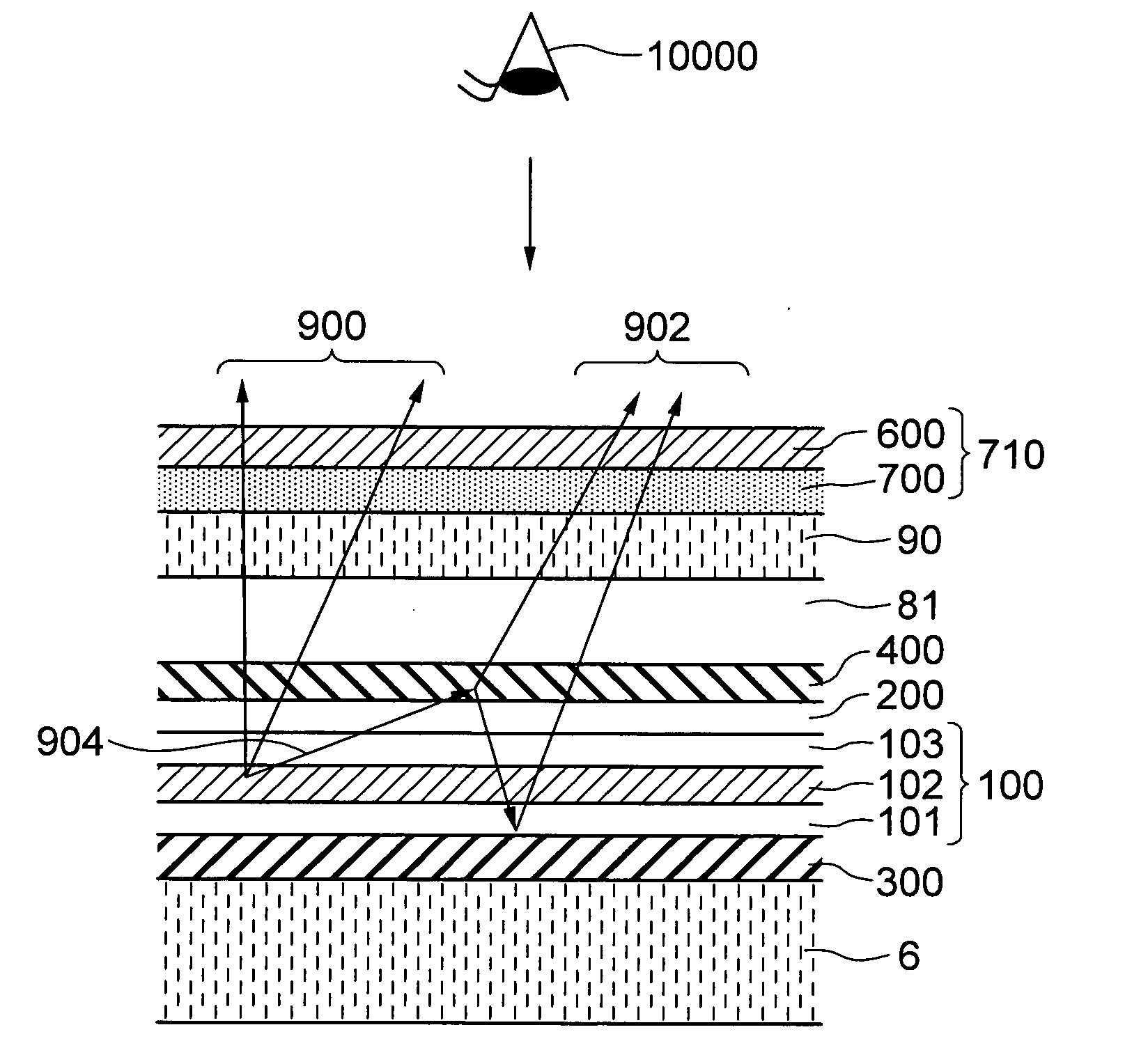
[0044]FIG. 1 shows a cross section of one Embodiment of a light-emitting device according to this invention.

[0045] The light-emitting device of this Embodiment is a so-called top-emission type organic light-emitting diode (hereinafter referred to as an OLED) that emits light from a side or surface opposite a substrate 6. An organic layer 100 making up the OLED is formed on a reflective electrode 300 that is formed over the substrate 6 and also serves as a reflective layer. A transparent electrode 200 is formed over the organic layer 100. Applying a DC voltage between the transparent electrode 200 and the reflective electrode 300 to pass a current between them causes the organic layer 100 to emit light of a wavelength corresponding to a predetermined color. One of the transparent electrode 200 and the reflective electrode 300 works as an anode and the other as a cathode. Here, it is supposed that the transparent electrode 200 serves as the anode and the reflective electrode 300 as t...

embodiment 2

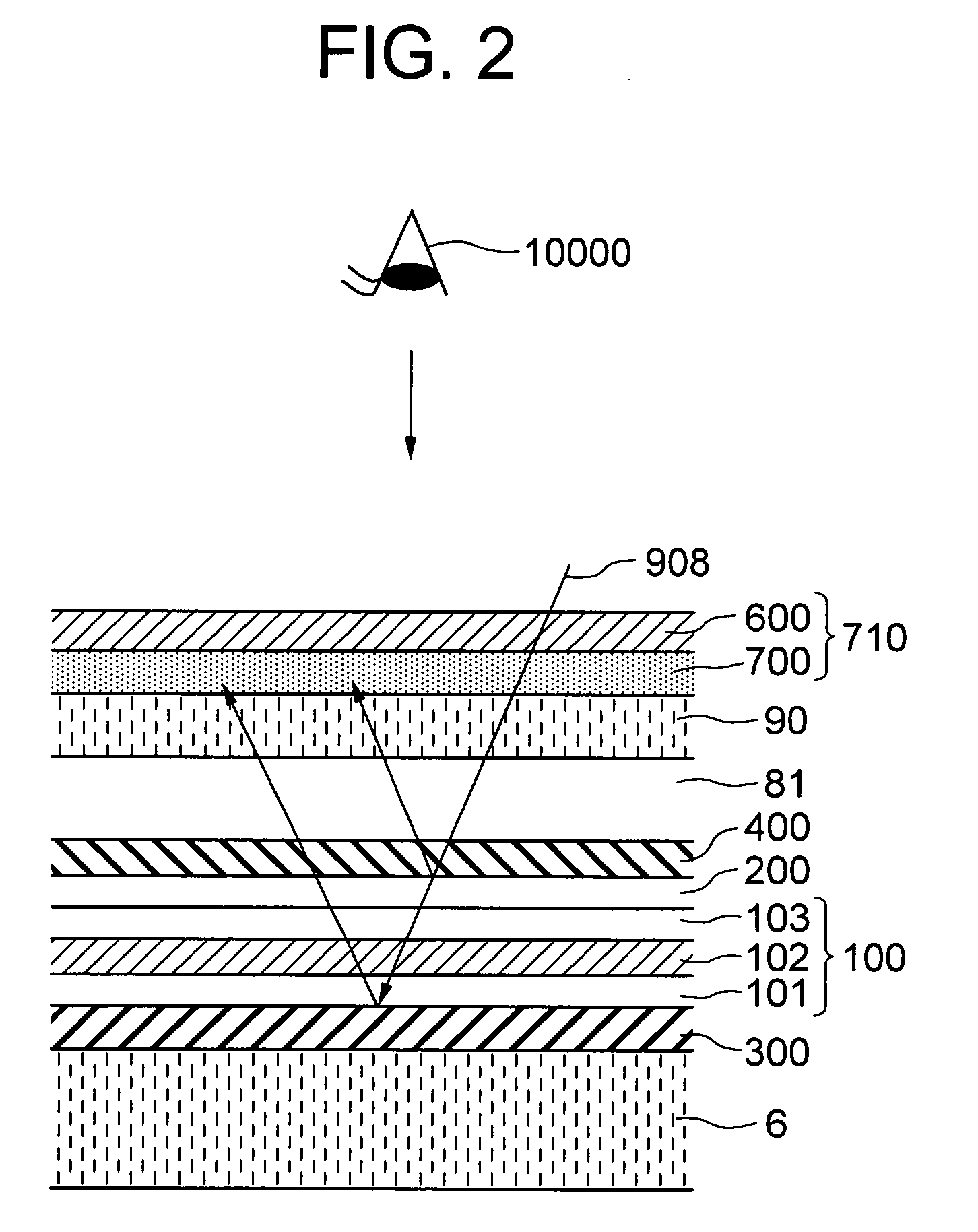
[0136]FIG. 8 is a cross-sectional view of a light-emitting device according to one Embodiment of this invention.

[0137] In the light-emitting device of this Embodiment, an organic layer 100 constituting an OLED device is formed over a reflective electrode 300, and a transparent electrode 200 is formed over the organic layer 100. Over the transparent electrode 200 are formed a high refractive index layer 502 and a nano-structure layer 400 that functions as a light extraction layer. The organic layer 100 is hermetically sealed by a transparent sealing plate 90, with a gap 81 formed between the transparent sealing plate 90 and the nano-structure layer 400. On the transparent sealing plate 90 is provided a circular polarizer 710 which prevents ambient light 908 reflected by the reflective electrode 300 and interfaces from coming out. When the light-emitting devices of this Embodiment are used in an emissive type display, a contrast reduction can be prevented.

[0138] The nano-structure l...

embodiment 3

[0147]FIG. 9 shows a cross section of a light-emitting device as one Embodiment of this invention.

[0148] The light-emitting device of this Embodiment has formed on the reflective electrode 300 an organic layer 100 constituting an organic light-emitting diode (OLED), on which a transparent electrode 200 is formed. Further, over the transparent electrode 200 is formed a rodlike nano-structure layer 402 that functions as a light extraction layer. The organic layer 100 is hermetically sealed with a transparent sealing plate 90, with a gap 81 formed between the transparent sealing plate 90 and the rodlike nano-structure layer 402. On the transparent sealing plate 90 is arranged a circular polarizer 710 that prevents ambient light 908 reflected by the reflective electrode 300 from going out of the device and thereby minimizes a reduction in contrast when the light-emitting device of this Embodiment is used in the OLED display.

[0149] The rodlike nano-structure layer 402 of this Embodimen...


PUM

PropertyMeasurementUnit
Thicknessaaaaaaaaaa
Diameteraaaaaaaaaa
Diameteraaaaaaaaaa

Abstract

A light-emitting device which is manufactured by a simple manufacturing method and which efficiently extracts light emitted from an emissive layer outward to improve the light extraction efficiency. The light-emitting device comprises a first electrode, a second electrode and an emissive layer disposed between them and extracts a part of light emitted from the emissive layer as radiated light. In this light-emitting device, the first electrode, the nano-structure layer for extracting the radiated light, and a gap having a refractive index lower than an average refractive index of the emissive layer and a nano-structure layer, are arranged in that order in a direction in which the radiated light is extracted.

Description

BACKGROUND OF THE INVENTION [0001] The present invention relates to a light-emitting device, an emissive type display having a plurality of the light-emitting devices arranged in matrix and controlling their light emitting operation for displaying an image, and an illumination device using the light-emitting devices. [0002] An organic light-emitting diode (OLED) is a device which, when its emissive layer formed of an organic thin film is injected with holes and electrons, transforms an electric energy into a light energy to emit light. Unlike a non-emissive type display as represented by a liquid crystal display, an emissive type display having the organic light-emitting diodes as light-emitting devices (referred to as “OLED display”) is self-luminous and requires no auxiliary light source such as a backlight and therefore has an advantage of being thin and lightweight. The OLED display is characterized by a wide view angle and a high response speed. [0003] The OLED has a substrate ...

Claims


Application Information

Patent Timeline
IPC IPC(8): G09F9/30H01L27/32H01L51/50H01L51/00H01L51/52H05B33/00H05B33/02H05B33/12H05B33/14H05B33/22
CPCB82Y20/00B82Y30/00H01L27/3244H01L51/0034H01L51/0035H01L51/0037H01L2251/5369H01L51/0059H01L51/0084H01L51/5268H01L51/5275H01L51/5281H01L51/0038H10K59/12H10K85/10H10K85/111H10K85/1135H10K85/114H10K85/631H10K85/341H10K50/854H10K50/858H10K50/86H10K2102/331A63F7/24A63F2007/341
Inventor SUGITA, TATSUYAADACHI, MASAYASASAKI, HIROSHI
Owner SAMSUNG DISPLAY CO LTD
Why Eureka
Try Eureka