Local control of underfill flow on high density packages, packages and systems made therewith, and methods of making same

Active Publication Date: 2005-09-08
INTEL CORP
View PDF4 Cites 23 Cited by
  • Summary
  • Abstract
  • Description
  • Claims
  • Application Information

AI Technical Summary

Problems solved by technology

The extent of this organic material flow, restricts the proximity of electrical contacts for passive components that are to be placed near the die, because the organic material can foul their contacts.

Method used


Image

  • Local control of underfill flow on high density packages, packages and systems made therewith, and methods of making same
  • Local control of underfill flow on high density packages, packages and systems made therewith, and methods of making same
  • Local control of underfill flow on high density packages, packages and systems made therewith, and methods of making same

Examples


Embodiment Construction

[0016] The following description includes terms, such as “upper”, “lower”, “first”, “second”, etc. that are used for descriptive purposes only and are not to be construed as limiting. The embodiments of a device or article described herein can be manufactured, used, or shipped in a number of positions and orientations. The terms “die” and “processor” generally refer to the physical object that is the basic workpiece that is transformed by various process operations into the desired integrated circuit device. A die is usually singulated from a wafer, and wafers may be made of semiconducting, non-semiconducting, or combinations of semiconducting and non-semiconducting materials. The term “chip” as used herein refers to a die that has been encapsulated in an organic, an inorganic, or a combination organic and inorganic housing. A “board” is typically a resin-impregnated fiberglass structure that acts as a mounting substrate for the chip.

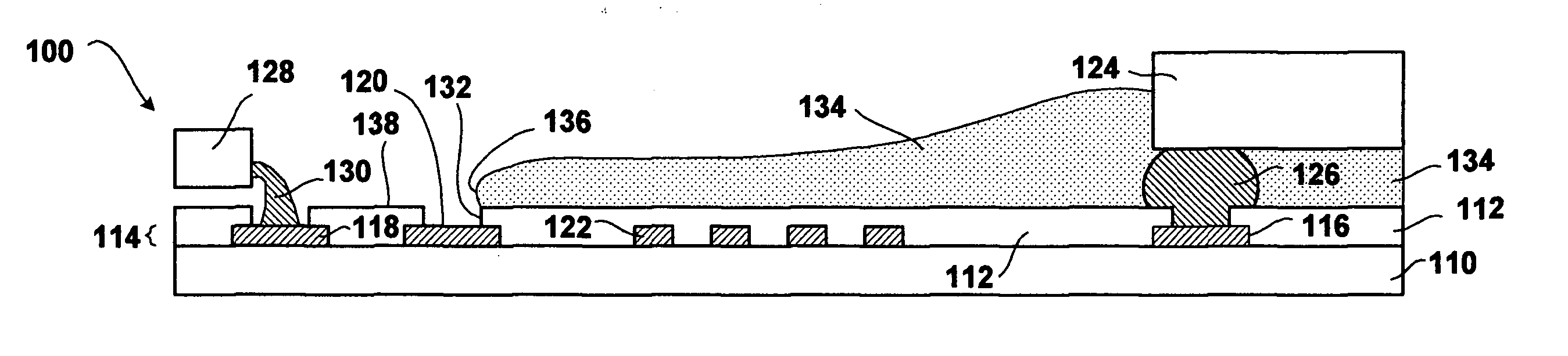
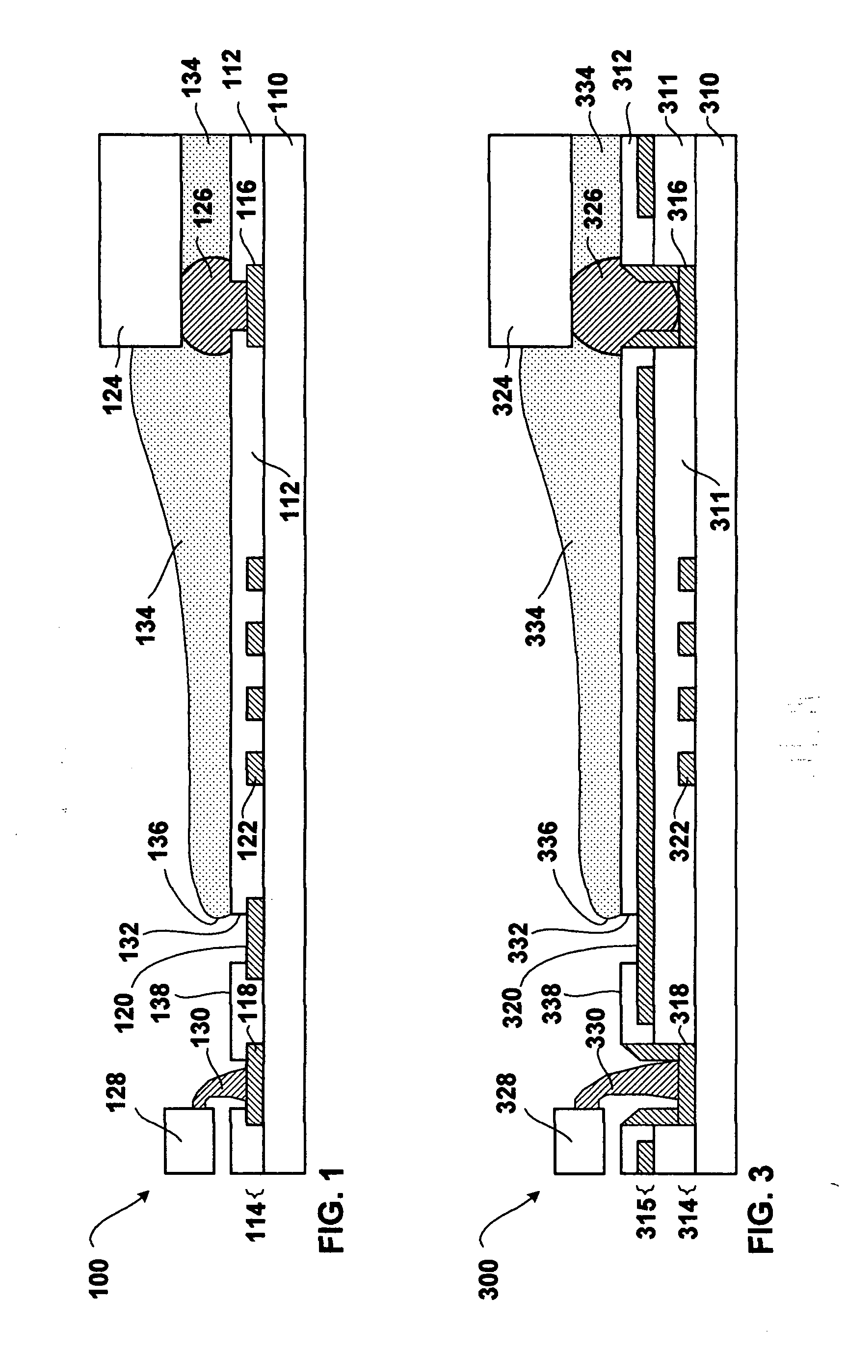
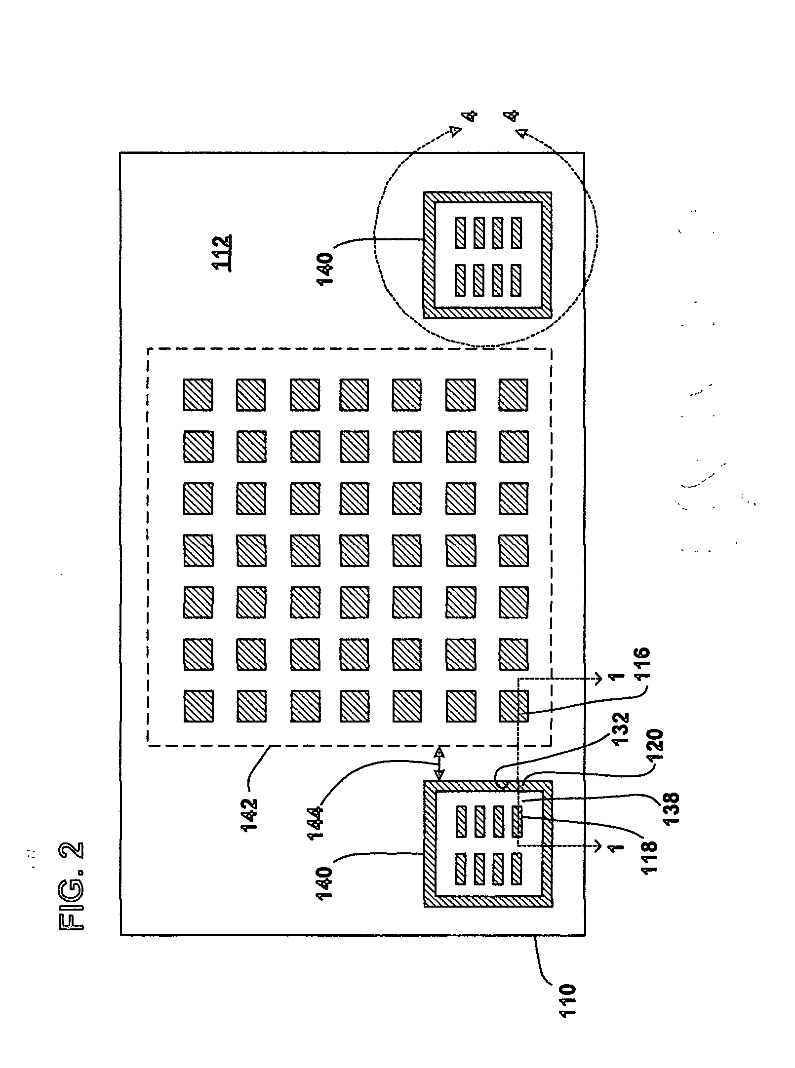
[0017]FIG. 1 is a cross-section of a package 100...


PUM

PropertyMeasurementUnit
distanceaaaaaaaaaa
distanceaaaaaaaaaa
distanceaaaaaaaaaa

Abstract

An article includes a mounting substrate, a passive component site on the mounting substrate, and an active component site on the mounting substrate. The article also includes a fluid flow barrier disposed local to the passive component site and spaced apart from the active component site. The fluid flow barrier can be a recess that resists fluid flow thereinto because of surface tension of the fluid when it meets the recess edge. The fluid flow barrier can include a boundary that diverts fluid flow due to the angle of the recess edge as the fluid approaches it. An embodiment also includes a packaging system that includes the article and at least one passive component. An embodiment also includes a method of assembling the article or the packaging system.

Description

TECHNICAL FIELD [0001] Embodiments relate to a packaged semiconductive die with integrated circuitry. More particularly, an embodiment relates to an underfill material flow barrier that is local to a passive component. BACKGROUND INFORMATION [0002] The thermal stability of packaging compositions such as underfill materials or other organic encapsulation molding compounds, is important in reducing the warpage of chip packages. Desirable materials have properties such as high thermal stability, low shrinkage, a favorable coefficient of thermal expansion (CTE), and other qualities such as a low moisture uptake. [0003] In chip packaging technology, the die is often bond-strengthened to the mounting substrate with an organic material that is flowed into contact with the die and the mounting substrate. In flip-chip processing, the organic material flows between the die active surface and the mounting substrate, thus strengthening the bond therebetween, while protecting the electrical cont...

Claims


Application Information

Patent Timeline
Patent Type & Authority Applications(United States)
IPC IPC(8): H05K7/06
CPCB23K1/0016Y10T29/49146B23K3/08B23K2201/42H01L21/563H01L24/13H01L24/16H01L24/32H01L24/73H01L24/83H01L25/18H05K3/284H01L2224/131H01L2224/16227H01L2224/16237H01L2224/26175H01L2224/32225H01L2224/73204H01L2224/83385H01L2924/1433H01L2924/14335H01L2924/19041H01L2924/19042H01L2924/19043H01L2924/19105H05K2201/10674H05K2201/10977B23K3/0623H01L2224/16225H01L2924/01029H01L2924/014H01L2924/00H01L2924/181H01L2924/14B23K2101/42
Inventor LANDEROS, JUANZHANG, JASONWANG, LEJUN
Owner INTEL CORP
Why Eureka
Try Eureka