Method for manufacturing semiconductor integrated circuit device

a semiconductor integrated circuit and manufacturing method technology, applied in semiconductor devices, semiconductor/solid-state device details, electrical devices, etc., can solve the problem of more difficult to maintain a long tddb lifetime, and achieve the effect of improving the dielectric breakdown strength

Inactive Publication Date: 2005-09-08
RENESAS TECH CORP
View PDF7 Cites 16 Cited by
  • Summary
  • Abstract
  • Description
  • Claims
  • Application Information

AI Technical Summary

Benefits of technology

[0005] An object of the present invention to provide a technique capable of improving dielectric breakdown strength between interconnects each using copper as a main conductor film.

Problems solved by technology

The insulating film having a low dielectric constant usually has a low dielectric breakdown, so that use of it has made it more difficult to maintain a long TDDB lifetime.

Method used


Image

  • Method for manufacturing semiconductor integrated circuit device
  • Method for manufacturing semiconductor integrated circuit device
  • Method for manufacturing semiconductor integrated circuit device

Examples


embodiment 1

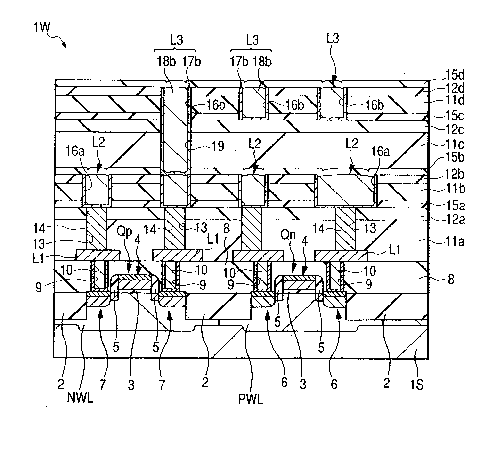
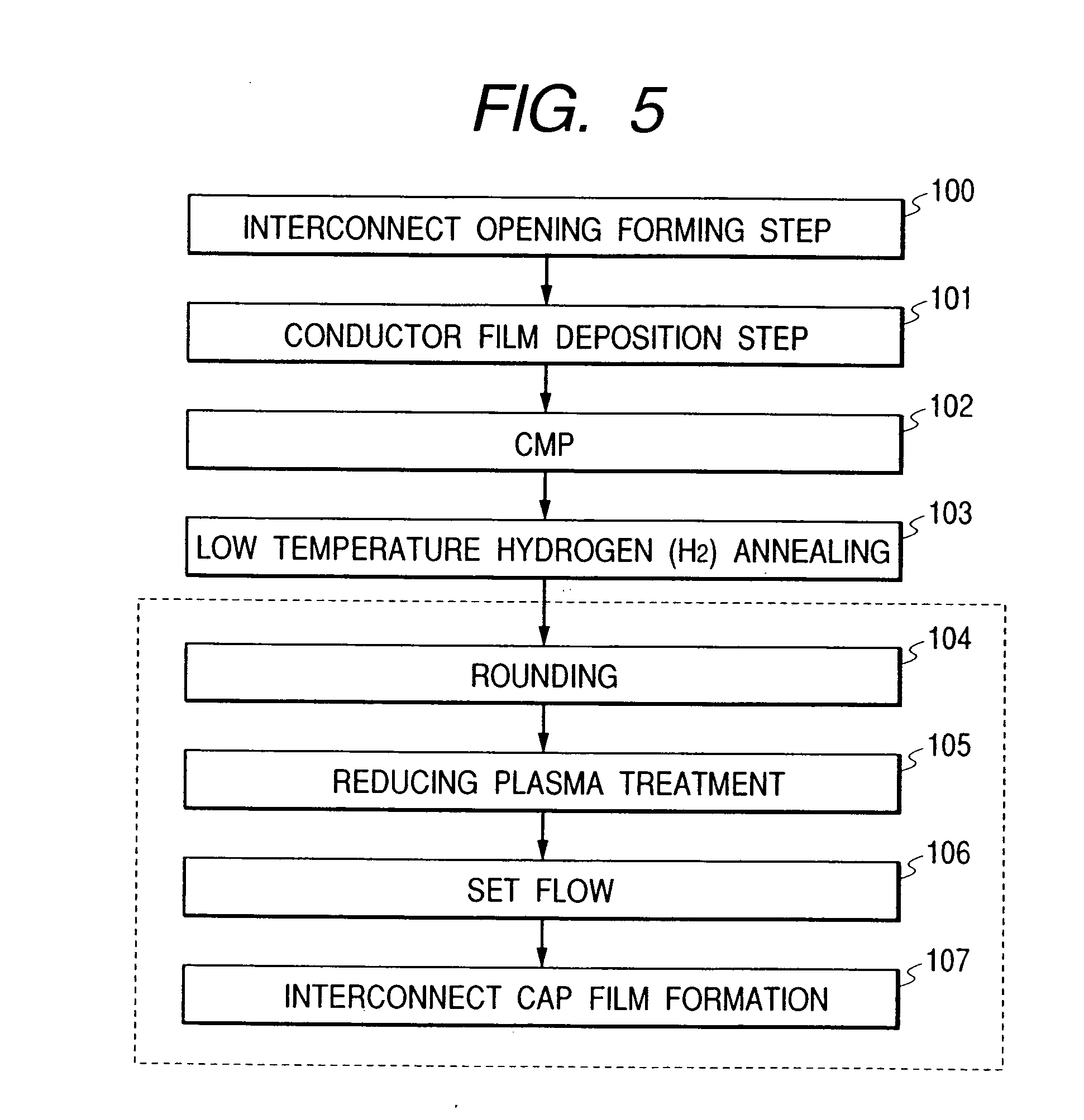
[0199] In this Embodiment, based on FIGS. 6 to 18 in accordance with the production flowchart of FIG. 5, explanation is made on the case where the technical idea of the present invention is applied to a manufacturing method of a CMIS (Complimentary MIS)-LSI (Large Scale Integrated Circuit). The step encompassed with a dotted line in FIG. 5 shows the treatment in the same treating chamber.

[0200]FIG. 6 is a fragmentary plane view of a CMIS-LSI during its manufacturing step and FIG. 7 is a cross-sectional view taken along a line X1-X1 of FIG. 6. A semiconductor substrate 1 (which will hereinafter be called substrate” simply) constituting a wafer 1W is made of p-type single crystal silicon having a specific resistance of about 1 to 10 Ωcm. The semiconductor substrate 1 has, on the main surface (surface on which a device is to be formed) thereof, an isolating trench (SGI (Shallow Groove Isolation) or STI (Shallow Trench Isolation)) 2. This isolation trench 2 is formed by embedding, for ...

embodiment 2

[0241]FIG. 19 is a flowchart of the manufacturing step of the semiconductor device according to another embodiment of the present invention. In this Embodiment 2, as illustrated in FIG. 19, the round taper of the main conductor film of the inlaid interconnect is formed in the set flow step 106. Described specifically, when the interconnect capping insulating film is made of a silicon nitride film, a silicon carbide film, an SiCN film or a silicon oxynitride film, a carrier gas such as nitrogen or helium is fed prior to feeding of a treatment gas upon set flow. While the time from the starting of feeding with the carrier gas until the starting of feeding with the treatment gas is set longer than that of the ordinary set flow, annealing is conducted during the introduction term of only the carrier gas, and stage temperature is set at a temperature as described in Embodiment 1, the wafer 1W is subjected to annealing treatment similar to that described in the round formation step of Emb...

embodiment 3

[0242] In Embodiment 3, a description will be made on the formation of an interconnect capping insulating film as a multilevel film. The insulating film is formed as a multilevel film in order to dissolve the problem discovered for the first time by the present inventor that when an SiON film such as the above-described “PE-TMS” (product of Canon) is employed as an interconnect capping insulating film, the conductive barrier film is inevitably oxidized upon formation of the insulating film. FIG. 20 is a fragmentary cross-sectional view of a semiconductor device, during its manufacturing process, according to a further embodiment of the present invention.

[0243] Upon deposition of an interconnect capping insulating film (second insulating film) 15b by CVD over the upper surface of the inlaid second-level interconnect L2 and insulating film 12b after the above-described ammonia plasma treatment without release of the chamber to the air, the insulating film 15b is deposited in order to...


PUM


Abstract

Provided is a manufacturing method of a semiconductor device which comprises (a) depositing a first insulating film over a wafer, (b) forming an interconnect opening in the first insulating film, (c) forming, in the interconnect opening, an interconnect having a conductor film comprised mainly of copper, (d) forming a taper at a corner of said conductor film on the opening side of the interconnect opening, and (e) depositing a second insulating film over the first insulating film and interconnect. The present invention makes it possible to improve dielectric breakdown strength between interconnects each having a main conductor film comprised mainly of copper.

Description

BACKGROUND OF THE INVENTION [0001] The present invention relates to a method for manufacturing a semiconductor device and a semiconductor device technique, particularly to a technique effective when adapted to a method for manufacturing a semiconductor device having an inlaid interconnect containing a main conductor film comprised mainly of copper and such a semiconductor device. [0002] An inlaid interconnect structure is formed by embedding a wiring material in an interconnect opening such as interconnect trench or hole formed in an insulating film in accordance with a metallization technique called “damascene technique” (single damascene and dual damascene techniques). When copper is employed as a main wiring material, however, it easily diffuses in an insulating film compared with a metal such as aluminum. Diffusion of copper from an inlaid interconnect to an insulating film is therefore suppressed or prevented by covering the surfaces (bottom surface and side surfaces) of the in...

Claims


Application Information

Patent Timeline
Patent Type & Authority Applications(United States)
IPC IPC(8): H01L21/28H01L21/02H01L21/314H01L21/3205H01L21/321H01L21/3213H01L21/768H01L23/52
CPCH01L21/02074H01L21/3144H01L21/3145H01L21/3148H01L21/3212H01L21/32136H01L21/76883H01L21/76826H01L21/76828H01L21/76832H01L21/76834H01L21/7684H01L21/76801H01L21/022H01L21/02263H01L21/02167H01L21/28
Inventor NOGUCHI, JUNJI
Owner RENESAS TECH CORP
Why Eureka
Try Eureka