Preferential ground and via exit structures for printed circuit boards

a printed circuit board and preferred ground technology, applied in the field of circuit board arrangement, can solve the problems of undesireable crosstalk between the signal paths of the transmission line or elecrical “noise”, affecting the integrity of electrically transmitted signals at high frequencies, and causing electromagnetic interference in the transmission lin

Inactive Publication Date: 2005-09-15
MOLEX INC
View PDF20 Cites 75 Cited by
  • Summary
  • Abstract
  • Description
  • Claims
  • Application Information

AI Technical Summary

Benefits of technology

[0014] A further object of the present invention is to provide an improved circuit board construction wherein a pair of differential signal vias are positioned proximate to an associated ground via, the circuit board having at least one ground plane layer formed therein, and the ground plane having an anti-pad formed therein that encompasses the two differential signal vias and which is connected to the associated ground via and another ground via associated with another pair of differential signal vias, and another anti-pad that is positioned adjacent to the one anti-pad and encompassing a second, adjacent pair of differential signal vias, but contacting a second ground via associated with the adjacent pair of differential signal vias.

Problems solved by technology

These devices have the potential to create electromagnetic interference in the transmission lines formed by the signal cables.
Large discontinuties in the impedance of the transmission line can lead to the generation of undesireable crosstalk between the signal paths of the transmission line or elecrical “noise”.
Both this type of noise and crosstalk adversely affect the integrity of electrically transmitted signals at high frequencies (or data transfer speeds).

Method used


Image

  • Preferential ground and via exit structures for printed circuit boards
  • Preferential ground and via exit structures for printed circuit boards
  • Preferential ground and via exit structures for printed circuit boards

Examples


Embodiment Construction

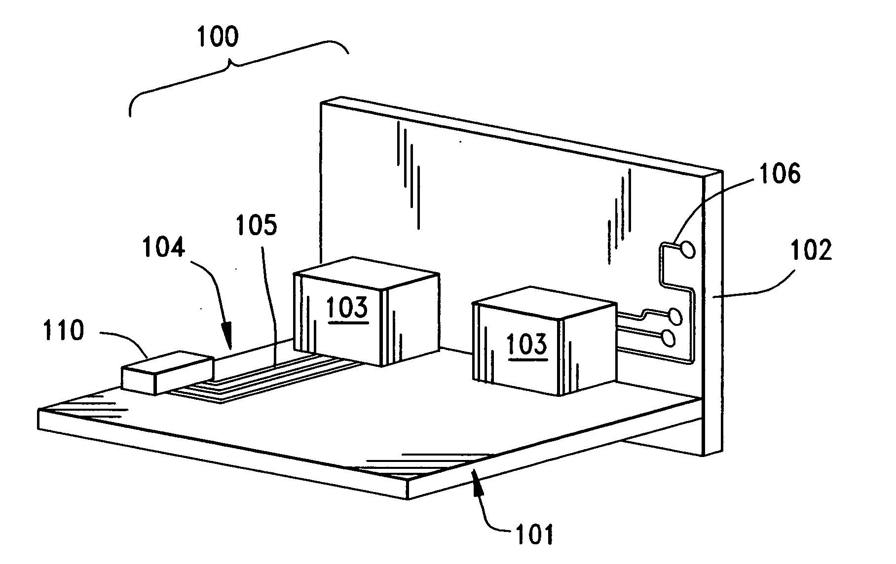
[0044]FIG. 1 is a perspective view of a backplane assembly 100 in which a printed circuit board, referred to herein as a “motherboard”101 is joined to a secondary circuit board 102 by way of one or more connectors 103. The connectors 103, as are known in the art, connect conductive circuits 104 which utilize conductive traces 105 disposed on a surface of the motherboard 101, to similar circuits 106 disposed on the secondary circuit board 102. These circuits 104, 106 typically lead to electronic components 110 that are mounted to the circuit board.

[0045] Cables may be used to connect the assembly 100 of FIG. 1 to another electronic assembly and these cables are but one form of an electronic signal transmission line. Other forms of such transmission lines may be incorporated in the circuit boards 104, 106 of the assembly and one such form may take the form of a plurality of conductive traces disposed on or within a plane, or layer, of the circuit board. An example of such a transmiss...


PUM


Abstract

A circuit board design is disclosed that is useful in high-speed differential signal applications uses either a via arrangement or a circuit trace exit structure. In the via arrangement, sets of differential signal pair vias and an associated ground are arranged adjacent to each other in a repeating pattern. The differential signal vias of each pair are spaced closer to their associated ground via than the spacing between the adjacent differential signal pair associated ground so that differential signal vias exhibit a preference for electrically coupling to their associated ground vias. The circuit trace exit structure involves the exit portions of the circuit traces of the differential signal vias to follow a path where they meet with and join to the transmission lines portions of the traces.

Description

REFERENCE TO RELATED APPLICATIONS [0001] This application claims priority of prior U.S. Provisional Patent Application No. 60 / 544,522, filed Feb. 13, 2004. BACKGROUND OF THE INVENTION [0002] The present invention relates generally to circuit board arrangements, and more particularly to via arrangements that are used on printed circuit boards for high-speed electrical transmission applications. [0003] In the field of data communication, data transfer speeds have steadily increased over the years. This increase in speed has required the development of high-speed electronic components for use in the telecommunications field, such as Internet use and use in data transfer and storage applications. In order to obtain an increase in the speed at which electrical signals are transmitted, it is known to use differential signals. [0004] Twisted pair wires are commonly used to transmit differential signals and are most commonly used in electrical cables. These signal cables have one or more tw...

Claims


Application Information

Patent Timeline
Patent Type & Authority Applications(United States)
IPC IPC(8): H01L23/64H01L23/66H01R12/16H01R12/51H01R13/658H05K1/02H05K1/11H05K3/42
CPCH01L2223/6627H01L2924/1903H01L2924/0002H05K1/0222H05K1/0245H05K1/0251H05K1/115H05K3/429H05K2201/044H05K2201/09236H05K2201/09609H05K2201/09636H05K2201/09718H05K2201/10189H01L2924/00H05K1/09
Inventor REGNIER, KENT E.BRUNKER, DAVID L.OGBUOKIRI, MARTIN U.
Owner MOLEX INC
Why Eureka
Try Eureka