Optical waveguide and production method thereof

a technology of optical waveguides and production methods, applied in the field of optical waveguides, can solve the problems of difficult to provide increased production efficiency, and the inability to define the optical waveguide between them in a stable form, so as to reduce the number of processes and time-consuming and complicated works involved in the interposition of spacers, reduce the contamination of the photo mask, and increase production efficiency

Inactive Publication Date: 2005-09-15
NITTO DENKO CORP
View PDF6 Cites 18 Cited by
  • Summary
  • Abstract
  • Description
  • Claims
  • Application Information

AI Technical Summary

Benefits of technology

[0009] It is the object of the present invention to provide a production method of an optical waveguide that can provide increased production efficiency and can also provide improved workability and production stability and provide an optical waveguide produced by the production method of the optical waveguide.
[0021] Thus, according to this method, the number of processes and time-consuming and complicated works involved in the interposition of the spacer can be reduced, thus providing increased production efficiency. In addition, even when the photo mask is put in contact with the resin layer, the contamination of the photo mask can be reduced. Further, since the resin layer is hard to flow, the optical waveguide can be formed in a stable form.
[0022] As a result of this, the optical waveguide of the present invention can be produced at reduced costs by virtue of the improved production efficiency and also can be applicable in various fields as the optical waveguide of high quality having excellent shape stability.

Problems solved by technology

However, the interposition of the spacer therebetween requires increased number of processes and time-consuming and complicated works, making it hard to provide increased production efficiency.
Further, the photosensitive resin in the liquid form provides the disadvantages that the mask can be contaminated by the resin in the handling and that owing to the fluidity of the resin, the optical waveguide cannot be defined therebetween in a stable form.

Method used


Image

  • Optical waveguide and production method thereof
  • Optical waveguide and production method thereof
  • Optical waveguide and production method thereof

Examples


example 1

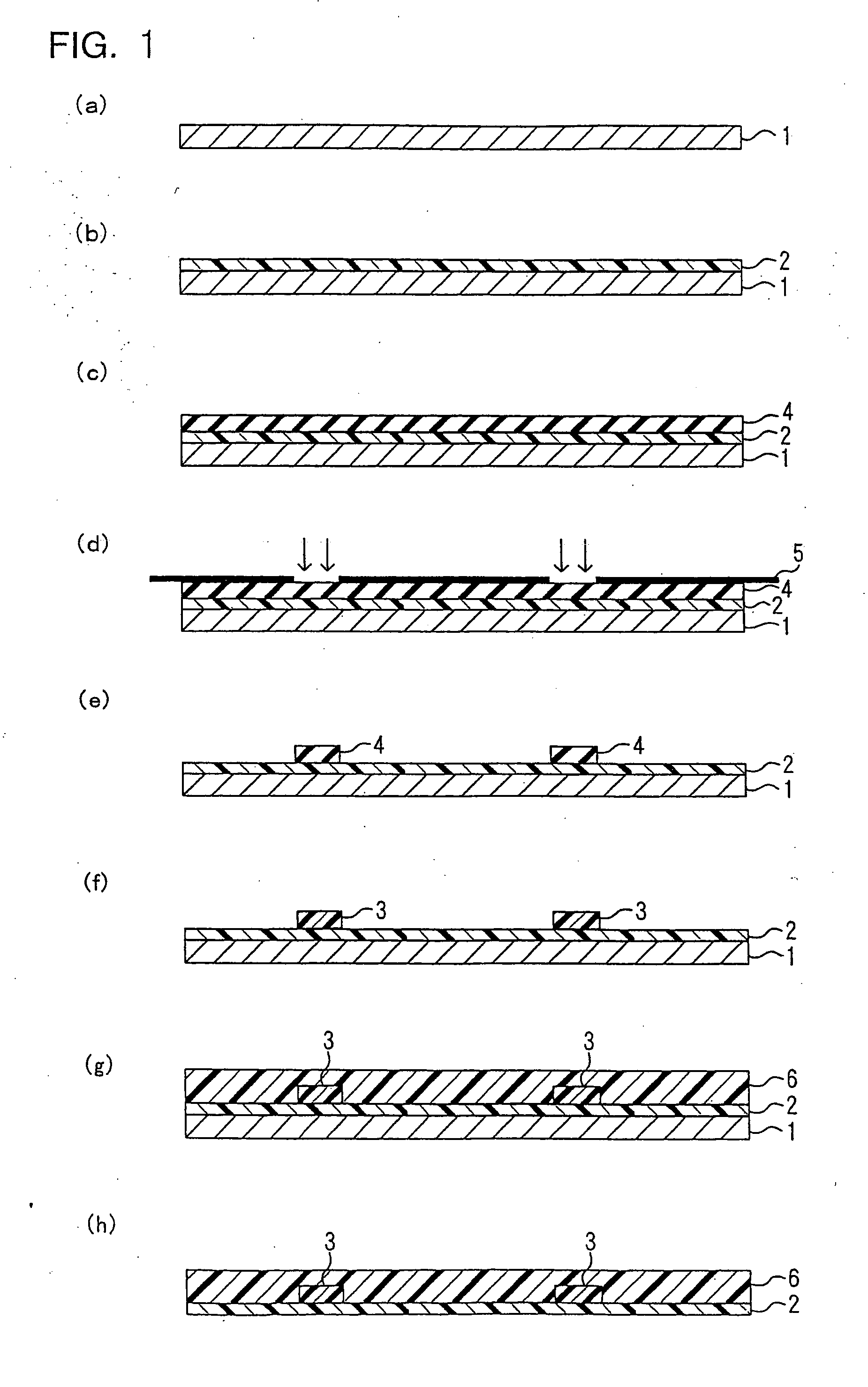
[0097] A substrate wherein an aluminum layer having a thickness of 20 nm was formed on a 10 cm×10 cm glass substrate by a vacuum deposition method was prepared(Cf FIG. 1(a)).

[0098] The varnish A was coated over the substrate by the spin coat method and then dried at 90° C. for 15 minutes, to form a resin layer. Thereafter, the whole area of the resin layer was irradiated with ultraviolet irradiation of 2,000 mJ / cm2 and then heated at 170° C. for 30 minutes, to form an under clad layer having a thickness of 30 μm (Cf. FIG. 1(b)).

[0099] Sequentially, the varnish B was coated over the under clad layer by the spin coat method and then dried at 90° C. for 15 minutes, to form a resin layer (Cf FIG. 1(c)). Then, the resin layer was irradiated with ultraviolet irradiation of 2,000 mJ / cm2 via a photo mask (an artificial quartz-based chromium mask) on which a linear optical waveguide pattern of 50 μm wide was depicted (Cf. FIG. 1(d)). At this time, the photo mask was put into direct contact...

example 2

[0105] Except that the varnish C was used as substitute for the varnish A, the same operation as in Example 1 was performed to form an under clad layer having a thickness of 30 μm on the substrate.

[0106] Sequentially, except that the varnish D was used as substitute for the varnish B, the same operation as in Example 1 was performed to form a core layer having a square-shaped section of 501 μm thick and 50 μm wide on the under clad layer.

[0107] At this time of exposure, the photo mask was put into direct contact with the resin layer, but no adhesion of the resin to the photo mask was found after the exposure of the resin layer to light.

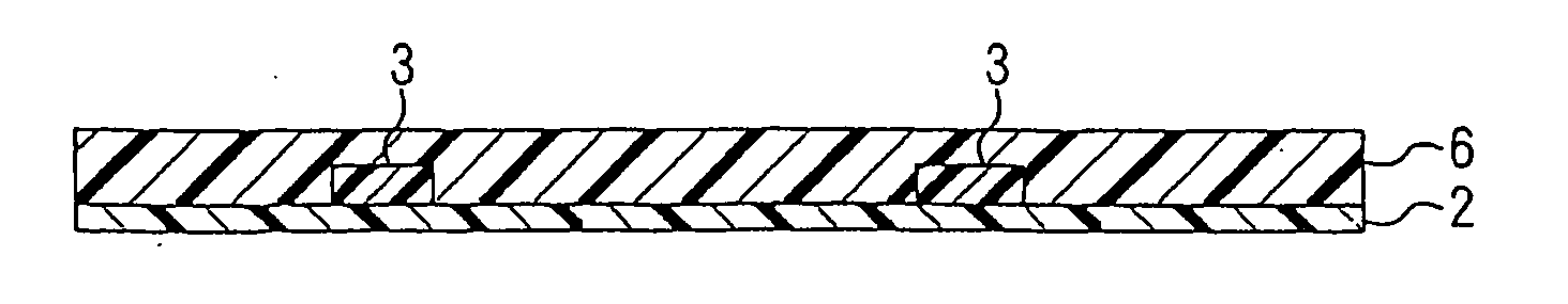
[0108] Thereafter, except that the varnish C was used as substitute for the varnish A, the same operation as in Example 1 was performed to form an over clad layer having a thickness of 80 μm. A multi-mode optical waveguide having a specific refractive index Δ of 3.0% was produced in the manner described above.

[0109] The substrate was not removed. ...

example 3

[0110] A 4-inch silicon wafer was prepared as the substrate, first. Then, the varnish E was coated over that substrate by the spin coat method and then was dried at 90° C. for 15 minutes, to form the resin layer. Thereafter, the whole area of the resin layer was irradiated with ultraviolet irradiation of 2,000 mJ / cm2 and then heated at 170° C. for 30 minutes, to form an under clad layer having a thickness of 10 μm.

[0111] Sequentially, except that the varnish F was used as substitute for the varnish B and the width of the pattern of the photo mask was changed to 6 μm, the same operation as in Example 1 was performed to form a core layer having a square-shaped section of 6 μm thick and 6 μm wide on the under clad layer.

[0112] At this time of exposure, the photo mask was put into direct contact with the resin layer, but no adhesion of the resin to the photo mask was found after the exposure of the resin layer to light.

[0113] Thereafter, except that the varnish E was used as substitu...


PUM

PropertyMeasurementUnit
thicknessaaaaaaaaaa
carbon numberaaaaaaaaaa
lengthaaaaaaaaaa

Abstract

A production method of an optical waveguide that can provide increased production efficiency and can also provide improved workability and production stability and provide an optical waveguide produced by the production method of the optical waveguide. A varnish comprising photopolymerizable resion composition comprising a fluorene derivative and a photoacid generator is coated over an under clad layer 2 and then is dried, to form a resin layer 4 having substantial no surface tack. Sequentially, the resin layer 4 is exposed to light in the state of being contacted with a photo mask 5 by a contact exposure method and then is developed, to form the resin layer 4 into a pattern. Thereafter, the resin layer 4 is cured to form a core layer 3 and then an over clad layer 6 is formed on the under clad layer 2 in such a manner as to cover the core layer 3, to thereby produce an optical waveguide. This method can allow the forming of the resin layer 4 having no surface tack, and as such can allow the use of the contact exposure to expose the resin layer to light. Hence, the number of processes and time-consuming and complicated works involved in the interposition of the spacer can be reduced, thus providing increased production efficiency.

Description

BACKGROUND OF THE INVENTION [0001] 1. Field of the Invention [0002] The present invention relates to an optical waveguide and to a production method thereof. More particularly, the present invention relates to an optical waveguide made by using polymer material and to a production method thereof [0003] 2. Description of the Prior Art [0004] An optical waveguide is widely used to optically connect a plurality of optical devices. In recent years, various attempts on the forming of this optical waveguide from polymer material to enhance the workability and the mass production have been considered. [0005] For example, JP Laid-open (Unexamined) Patent Publication No. Hei 10-268152 proposes that photosensitive resin in liquid form, such as epoxy oligomer and acrylic oligomer, is coated over an under clad layer, then is exposed to light through a mask, and then is developed with solvent, to form a pattern into a core layer. [0006] However, since the photosensitive resin mentioned above is ...

Claims


Application Information

Patent Timeline
Patent Type & Authority Applications(United States)
IPC IPC(8): G02B6/12C08G59/24G02B1/04G02B6/13
CPCG02B1/046G02B1/045
Inventor MUNE, KAZUNORIMOCHIZUKI, AMANESHIMIZU, YUSUKEKINJOU, NAOTAKA
Owner NITTO DENKO CORP
Why Eureka
Try Eureka