Method of manufacturing tape wiring substrate

a manufacturing method and technology of wiring substrate, applied in the direction of manufacturing tools, conductive material removal by irradiation, electric discharge removal of conductive materials, etc., can solve the problems of increasing production costs and difficulty in forming micro-scale wiring patterns with fine pitches on copper foil, so as to simplify the manufacturing process and reduce production costs

Inactive Publication Date: 2005-09-22
SAMSUNG ELECTRONICS CO LTD
View PDF9 Cites 5 Cited by
  • Summary
  • Abstract
  • Description
  • Claims
  • Application Information

AI Technical Summary

Benefits of technology

[0014] To solve the above-described problems, embodiments of the present invention provide a method of manufacturing a tape wiring substrate, by which production cost can be reduced by a simplified manufacturing process and a fine wiring pattern having fine pitches can be formed.

Problems solved by technology

So many processing steps give rise to an increase in the volume of a production line, and volumes of materials that are consumed regularly, for example, PR, PR developer, copper foil etchant or the like, become increased, thereby inevitably increasing the production cost.
Further, since the light source 132 having a relatively large wavelength of several hundreds of micrometers is used in the conventional photolithographic etching, it is quite difficult to form a micro scale wiring pattern having fine pitches on the copper foil 120.

Method used


Image

  • Method of manufacturing tape wiring substrate
  • Method of manufacturing tape wiring substrate
  • Method of manufacturing tape wiring substrate

Examples


Embodiment Construction

[0025] Advantages and features of the present invention and methods of accomplishing the same may be understood more readily by reference to the following detailed description of preferred embodiments and the accompanying drawings. The present invention may, however, be embodied in many different forms and should not be construed as being limited to the embodiments set forth herein. Rather, these embodiments are provided so that this disclosure will be thorough and complete and will fully convey the concept of the invention to those skilled in the art, and the present invention will only be defined by the appended claims. Like reference numerals refer to like elements throughout the specification.

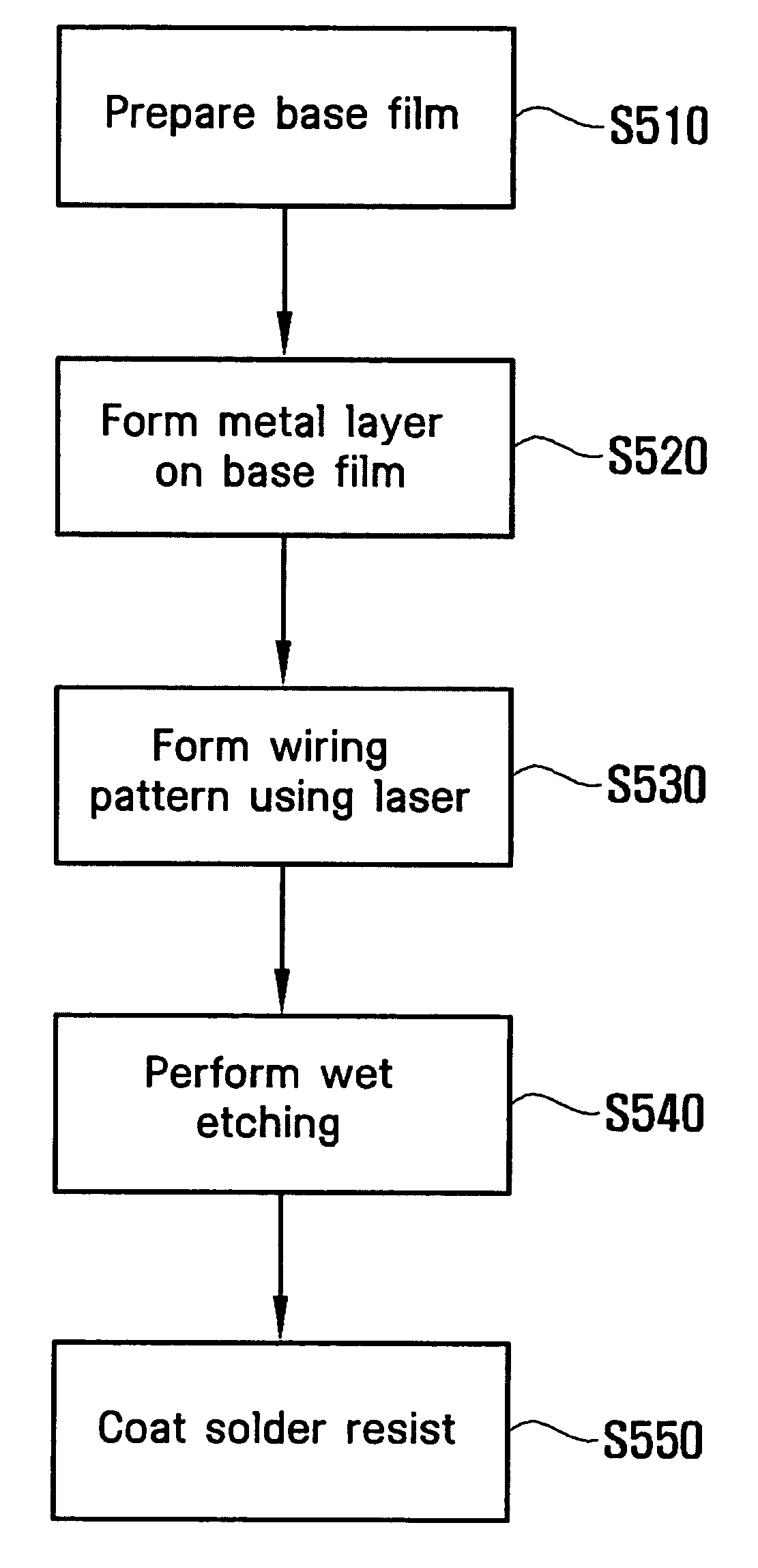
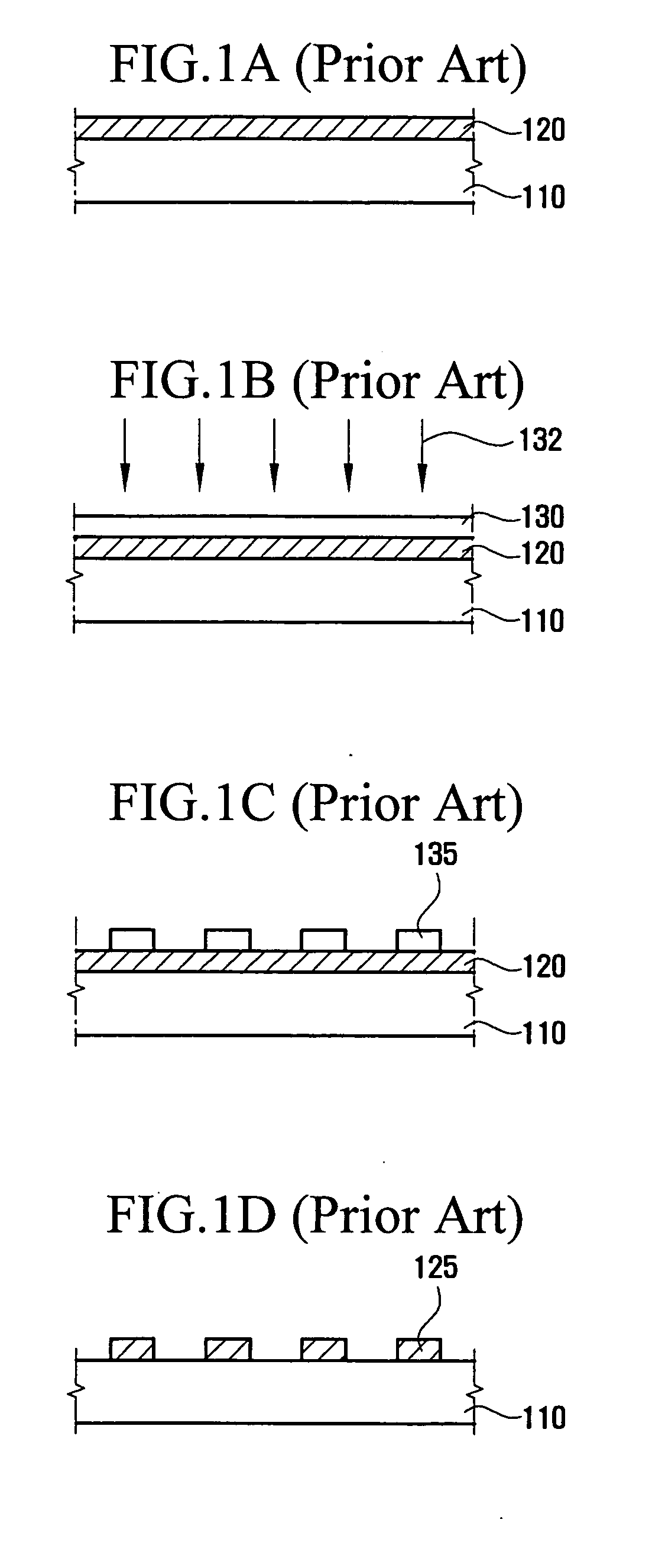
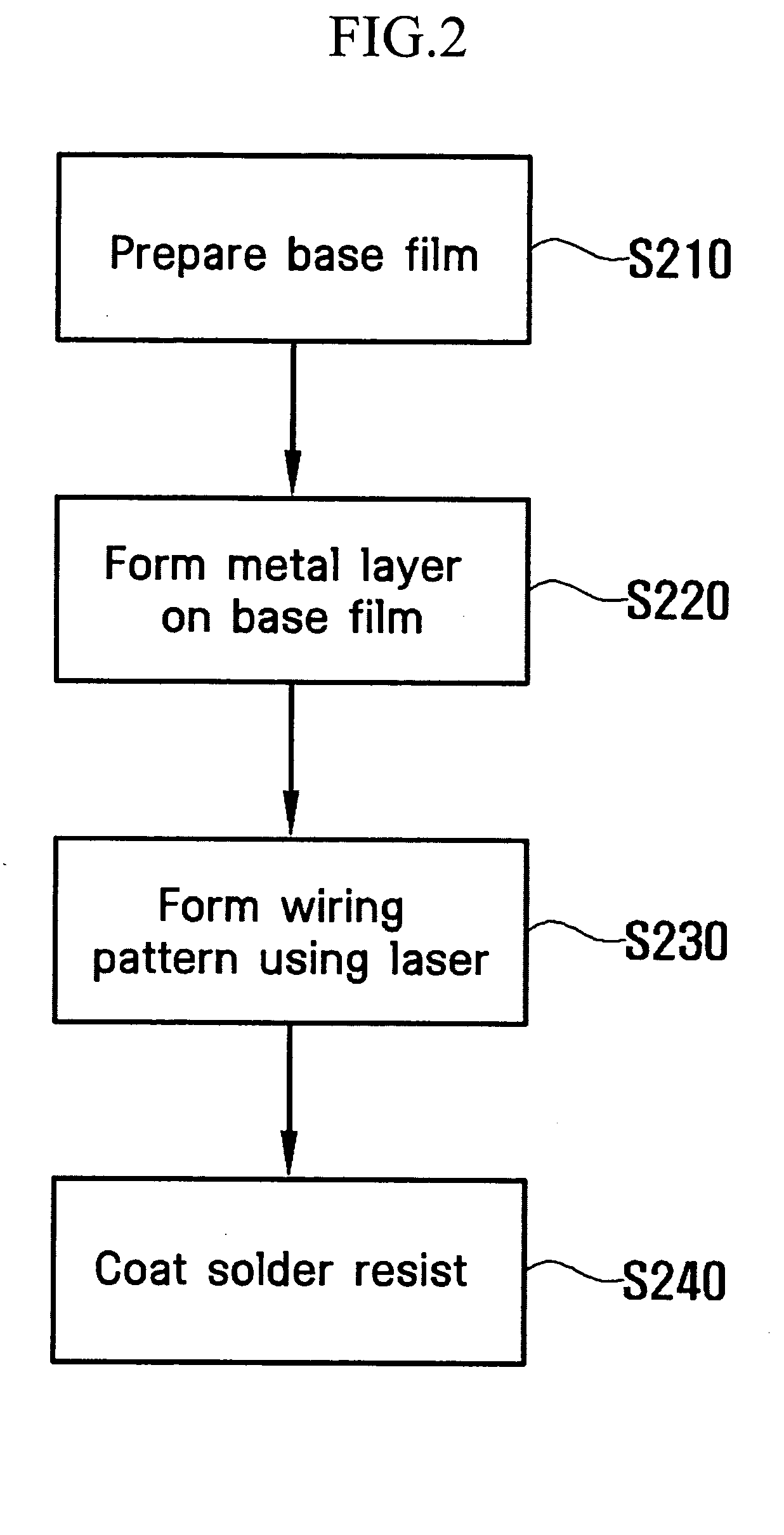
[0026] A flexible printed circuit board (FPC), such as a tape carrier package (TCP) or a chip on film (COF), in which a wiring pattern is formed on a base film, can be used as a tape wiring substrate in an embodiment of the present invention. The tape wiring substrate used in an embodiment...


PUM

PropertyMeasurementUnit
thicknessaaaaaaaaaa
thicknessaaaaaaaaaa
wavelengthaaaaaaaaaa

Abstract

A method of manufacturing a tape wiring substrate, by which the production cost can be reduced by a simplified manufacturing process. A fine wiring pattern having fine pitches can be formed. The method of manufacturing a tape wiring substrate includes preparing a base film, forming a metal layer on the base film, and processing the metal layer into a wiring pattern using a laser. In addition, the metal layer is partially removed using the laser, and a wiring pattern is formed by a subsequent wet etching.

Description

[0001] This application claims priority from Korean Patent Application No. 10-2004-0017943 filed on Mar. 17, 2004 in the Korean Intellectual Property Office, the disclosure of which is incorporated herein in its entirety by reference. BACKGROUND OF THE INVENTION [0002] 1. Field of the Invention [0003] The present invention relates to a method of manufacturing a tape wiring substrate, and more particularly, to a method of manufacturing a tape wiring substrate, by which a wiring pattern is formed using a laser. [0004] 2. Description of the Related Art [0005] According to a recent trend for thin, compact, highly integrated, high speed and multi-pin semiconductor devices, tape wiring substrates have been increasingly employed in techniques of mounting semiconductor chips. The tape wiring substrates are configured so that a wiring pattern layer is formed on a base film made of an insulating material such as polyimide resin. It is possible to apply a tape automated bonding (TAB) technique...

Claims


Application Information

Patent Timeline
Patent Type & Authority Applications(United States)
IPC IPC(8): B23K26/36B23K101/42C23F1/00C23F1/18C23F4/00C23F4/02H01L21/60H05K3/00H05K3/02H05K3/06H05K3/08H05K3/46
CPCC23F1/02C23F1/18C23F4/02H05K3/027H05K2203/1476H05K2203/0369H05K2203/0783H05K2203/1121H05K3/06H01L21/60
Inventor LEE, CHUNG-SUNKANG, SA-YOONKWON, YONG-HWANCHOI, KYOUNG-SEI
Owner SAMSUNG ELECTRONICS CO LTD
Why Eureka
Try Eureka