Method of sensor packaging

a sensor and packaging technology, applied in the field of flexible interconnection packaging system, can solve the problems of limiting the placement and arrangement of components within the housing, affecting the reliability of the connection, so as to achieve reliable connection

Inactive Publication Date: 2005-09-22
SOCIONEXT INC
View PDF8 Cites 26 Cited by
  • Summary
  • Abstract
  • Description
  • Claims
  • Application Information

AI Technical Summary

Benefits of technology

[0012] The present invention includes a flexible interconnect packaging system. The system makes use of a flexible printed circuit board as the main substrate material. In one embodiment, components are mounted or attached to the substrate using standard die attachment adhesive (conductive or non-conductive). Bonding pads of the components are connected to conductive trace pads of the flexible substrate using techniques such as, wire bonding, ball / bump methods, tape automated bonding (TAB), or any other applicable bonding methodology for integrated circuits. The packaging includes a plastic transfer molding in the form of a pre-molded package that provides physical support and protection, and enables reliable connection between the component and the substrate.
[0013] Using the packaging system included in the present invention provides several advantages over convention systems. In conventional systems, IC devices generally must follow the orientation of the main circuit board. However, the packaging system included in the present invention allows the circuit to bend, thus providing a way for devices to be placed in virtually any orientation. For example, a component may be located away from a main circuit board and orientated in virtually any orientation with regards to the main circuit board. For example, the component may be a fingerprint sensor that is used in a cell phone. The packaging system included in the present invention allows the fingerprint sensor to be located away from the main circuit board and orientated and exposed at an outside surface of the cell phone to provide the best sensor position for use by the cell phone user.
[0014] Furthermore, the packaging system allows devices to be coupled to the main circuit board via a single socket connector located on the circuit board, thereby providing easy access and quick connect and disconnect of the device from the circuit. This allows easy replacement by the user without the need to return the device to the manufacturer. The packaging system is applicable to all types of electronic devices, optical devices, touch / pressure devices and any other type of sensor or electrical component.
[0015] Thus, the limitations on sensor placement onto a given enclosure (cell phone, PDA and etc.) has been eliminated. For example, with the advantages offered by one or more embodiments of the present the invention, cell phone designers now have freedom to select the mounting location for sensor components at any location on the enclosure. Due to the easy connection and disconnection of the packaging system from the main circuit board, the sensor can be replaced either by the end user or at a field service location. Thus, the device does not have to be returned to a service center and users do not have to wait for days to repair the device.

Problems solved by technology

As a result, limitations exist as to where and how the components can be arranged within the housing and how they are presented at the external surface of the housing to the consumer.
One of the most important issues in electronic packaging is that of packaging and interconnecting integrated circuits (ICs).
Given the above-described packaging system it is easy to see that several limitations exist.
Furthermore, the technique results in size and flexibility limitations because the size of the circuit board 104 and the associated connectors (106, 114) limit how and where the component 102 may be located in a housing, and how such components are presented to the user at the outside surface of the device.

Method used


Image

  • Method of sensor packaging
  • Method of sensor packaging
  • Method of sensor packaging

Examples


Embodiment Construction

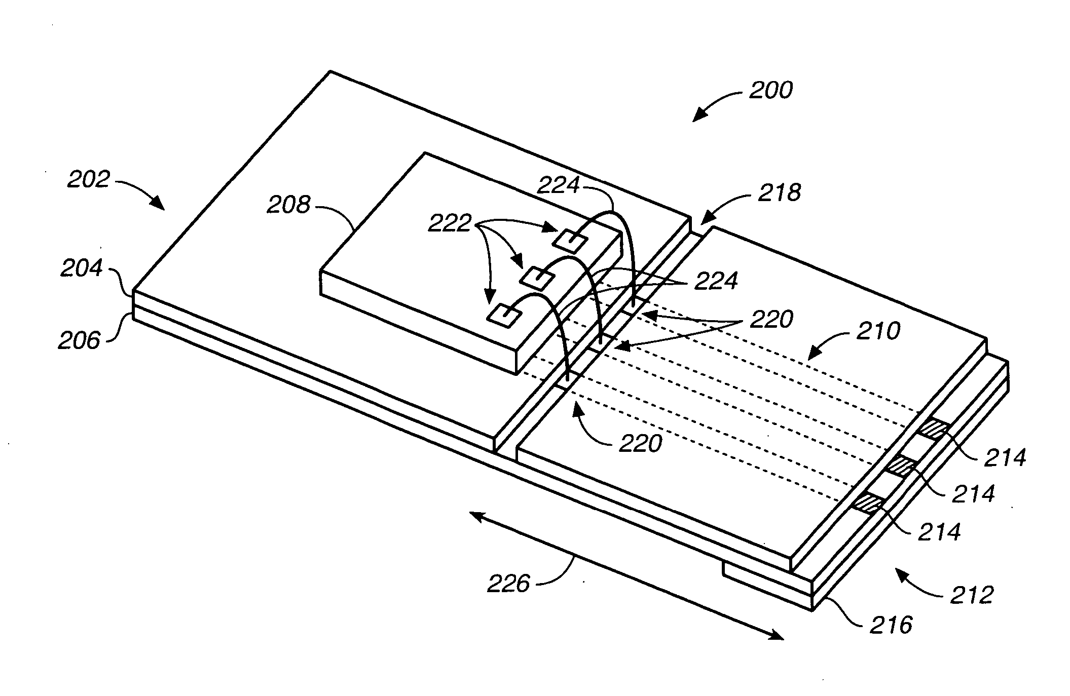
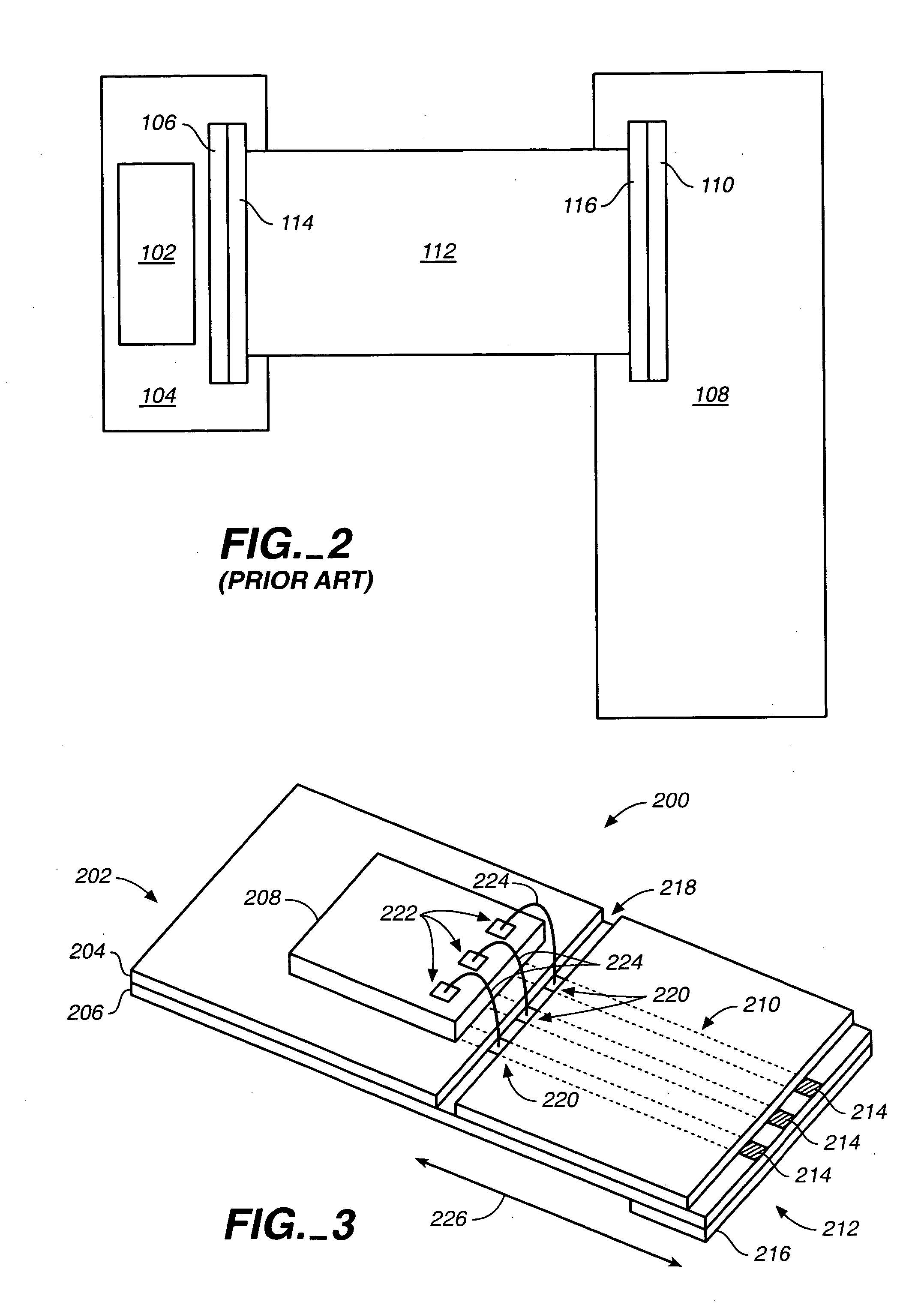
[0027] The present invention includes a flexible interconnect packaging system that overcomes the limitations of conventional packaging systems. For example, in one embodiment, a flexible packaging system is provided that includes a flexible substrate and a pre-molded or post-assembly molded plastic package that forms an open cavity for receiving a fingerprint sensor. Such a flexible packaging system can be used within the housing of a cellular telephone, or other portable electronic device, to provide the sensor at an outside surface of the device housing, while electrically coupling the sensor to an internal circuit board that has an orientation that is different from the sensor's orientation.

[0028] The packaging system as described above fits into very small form factor devices and is producible at a relatively low cost. Furthermore, the packaging system is easily replaceable in case of damage to the sensor. For example, the fingerprint sensor may be damaged by a hard material s...


PUM


Abstract

The present invention is directed to a method of making flexible interconnect packaging, in particular, packaging for fingerprint sensor chips. The chip is mounted on a flexible substrate having conductive traces leading to a connector at an end of the substrate. Wires are used to connect contact pads with the conductive traces, and a rigid frame is mounted below the substrate and chip. The conductive traces are preferably internal within the substrate and are exposed by forming a cavity in the substrate adjacent to the chip. Also disclosed are electronic devices which incorporate the foregoing fingerprint sensing apparatus.

Description

CROSS REFERENCE TO RELATED APPLICATIONS [0001] This application claims priority as a division of allowed U.S. patent application Ser. No. 10 / 160,438, published Dec. 4, 2003, (Pub. No. U.S. 2003 / 0224553-A1). This application also related to commonly owned U.S. Pat. No. 6,653,723, issued on Nov. 25, 2003, entitled “System For Providing An Open-Cavity Low Profile Encapsulated Semiconductor Package.” The disclosures of the above parent application and related patent are incorporated by reference.FIELD OF THE INVENTION [0002] The present invention relates to packaging systems, and more particularly, to a flexible interconnect packaging system. BACKGROUND OF THE INVENTION [0003] Given the reduced size of many consumer electronic devices, packaging systems are becoming increasingly important. For example, cellular telephones are becoming smaller and smaller to satisfy consumer's desires for portable lightweight telephones that are easy to carry. Such devices must still provide all the feat...

Claims


Application Information

Patent Timeline
Patent Type & Authority Applications(United States)
IPC IPC(8): H01L25/18G06K9/00H01L23/498H01L25/04
CPCG06K9/00053H01L23/3121H01L2924/10253H01L2924/1815H01L2924/15174H01L2924/14H01L2924/01079H01L2924/01078H01L2924/01077H01L2924/01029H01L2924/01014H01L2224/85444H01L2224/85205H01L23/4985H01L24/45H01L24/48H01L24/49H01L2224/45144H01L2224/48091H01L2224/48227H01L2224/48228H01L2224/48464H01L2224/49175H01L2924/00014H01L2924/00H01L2224/48644H01L2224/05553H01L2224/8592H01L2924/181G06V40/1329H05K1/14
Inventor MANANSALA, MICHAEL
Owner SOCIONEXT INC
Why Eureka
Try Eureka