Organic semiconductor device and method of producing the same

Inactive Publication Date: 2005-09-29
CANON KK
View PDF3 Cites 12 Cited by
  • Summary
  • Abstract
  • Description
  • Claims
  • Application Information

AI Technical Summary

Benefits of technology

[0010] According to the present invention, it is possible to provide an organic semiconductor device having good device characteristics and capable of incr

Problems solved by technology

However, an organic semiconductor differs from an inorganic semiconductor, and behaviors of the organic semiconductor are hardly

Method used


Image

  • Organic semiconductor device and method of producing the same
  • Organic semiconductor device and method of producing the same
  • Organic semiconductor device and method of producing the same

Examples


Example

EXAMPLE 1

[0032] The concept and embodiment of the present invention are described referring to FIGS. 1 to 5.

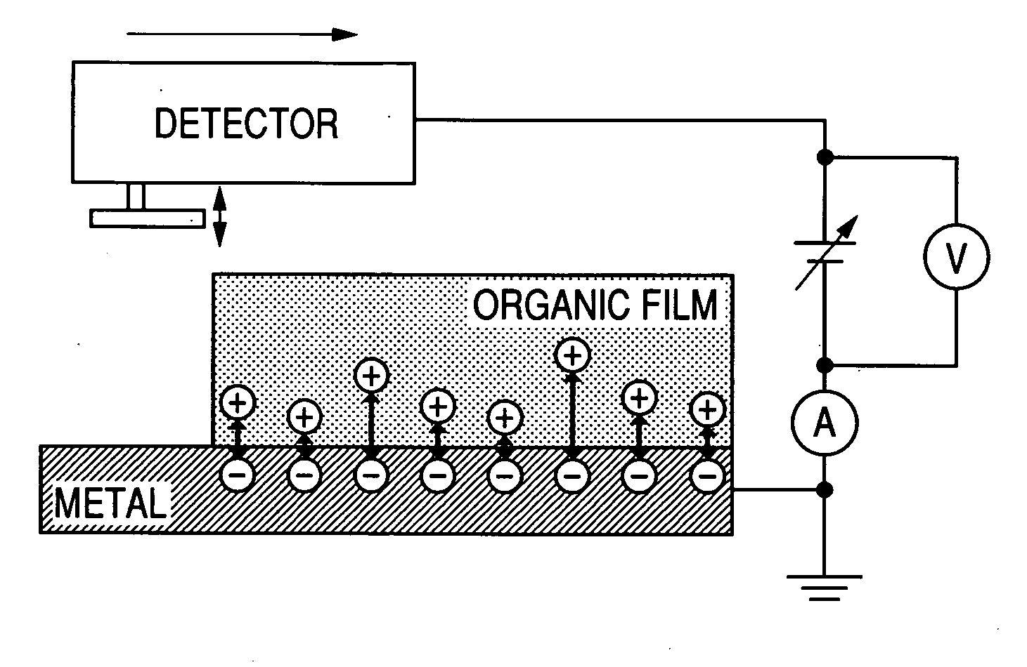
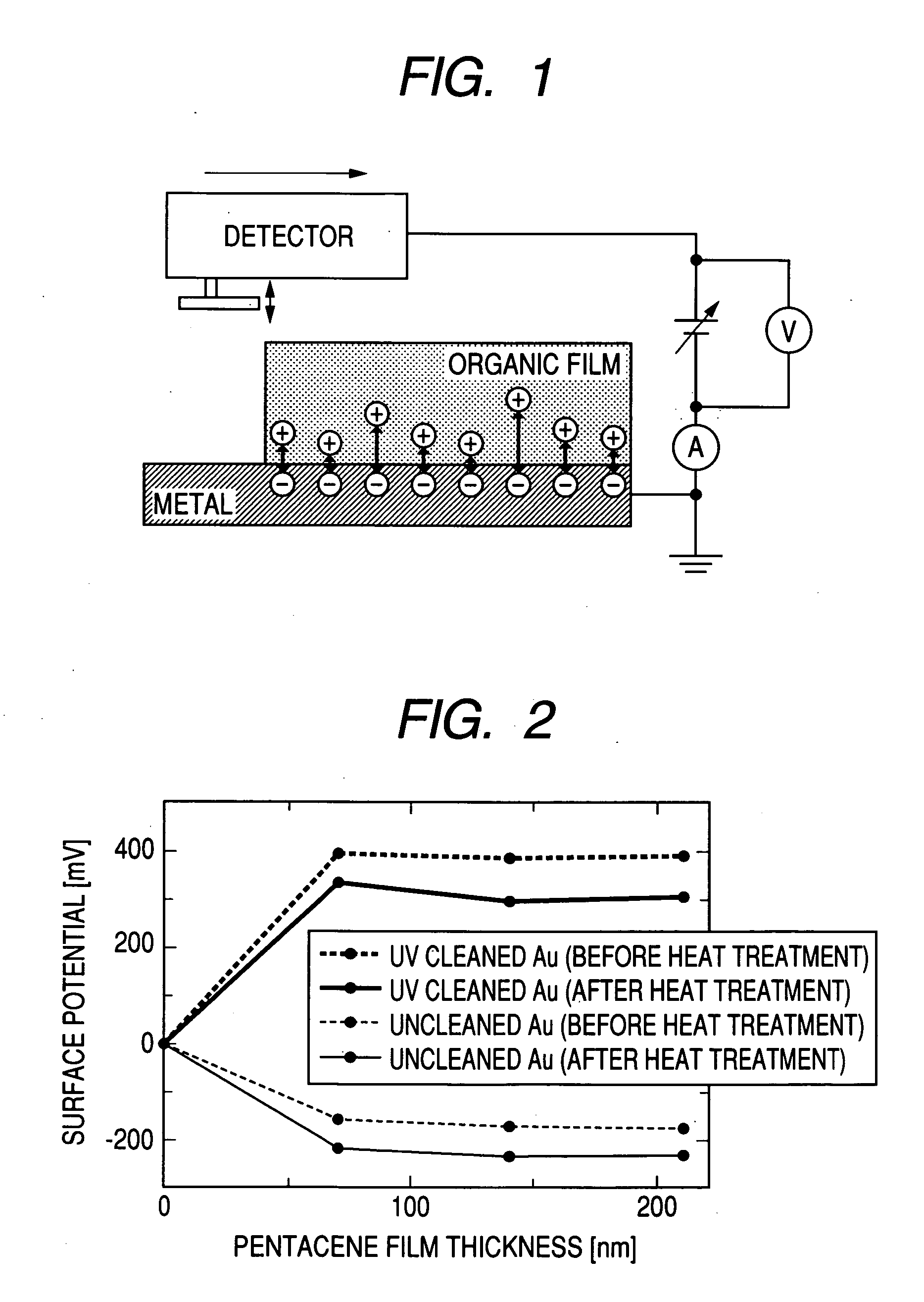
[0033]FIG. 1 is a schematic diagram explaining measurement of an electrostatic potential generated at a surface of an organic semiconductor using a sample prepared by contacting a conductive electrode and an organic semiconductor material. A metallic thin film was used as a conductive material and was connected to the ground. A change in surface potential was measured by scanning from the surface of the metal to the surface of the organic semiconductor material using a Kelvin probe detector (probe).

[0034]FIG. 2 shows an example of the results of the surface potential measurement. A gold thin film was used as a conductive electrode material, and an vacuum-evaporated pentacene was used as an organic semiconductor material. Ultraviolet (UV) irradiation and heat treatment were used as adjustment means. A relationship between a surface electrostatic potential of the pentacene fi...

Example

EXAMPLE 2

[0039] Similar effects were obtained by employing DC plasma exposure in a 0.5 Pa argon atmosphere as the adjustment means.

Example

EXAMPLE 3

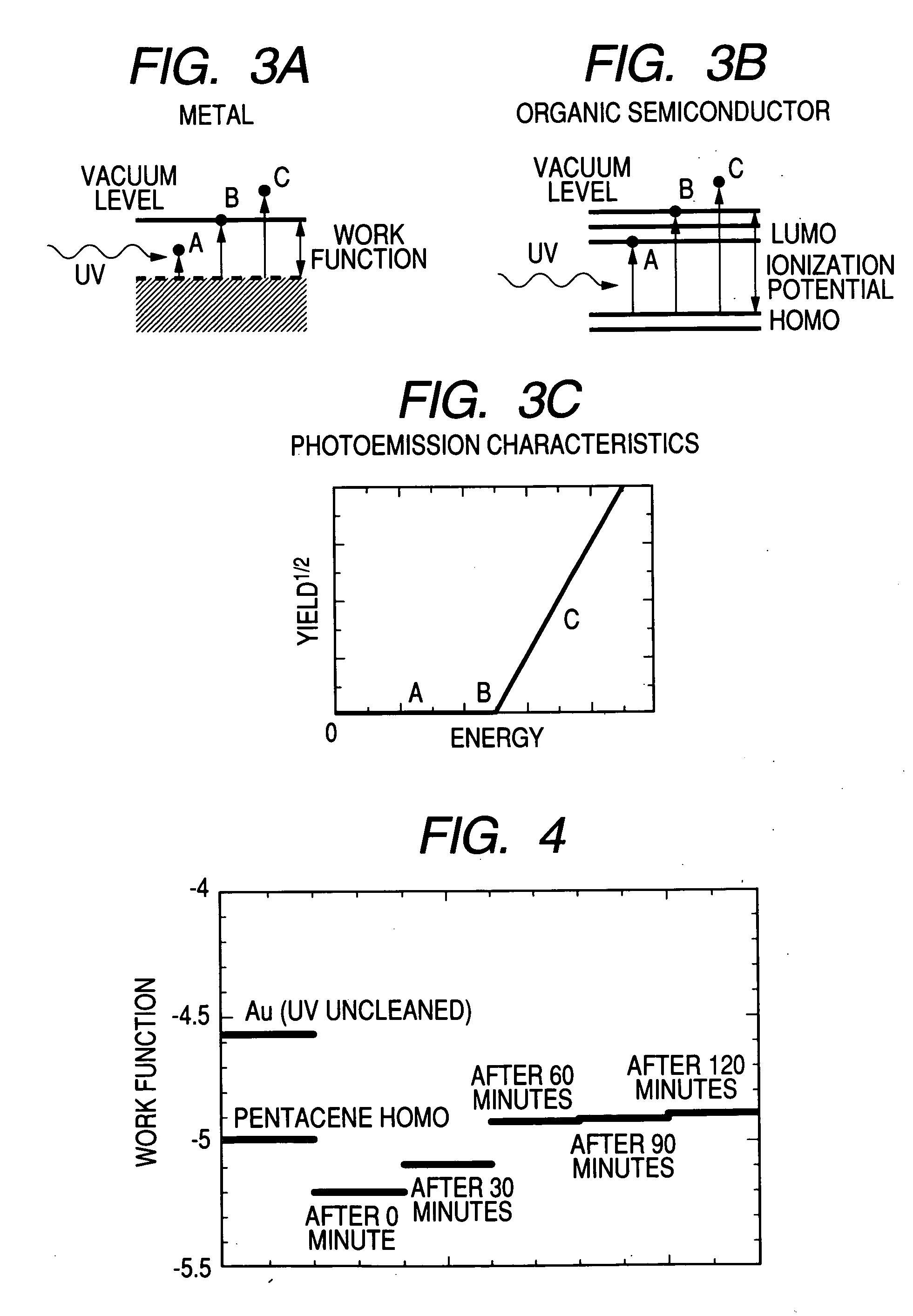
[0040] The surface of a gold electrode was subjected to surface treatment with UV irradiation (UV cleaning) as the adjustment means. Then, an evaporated pentacene film (thickness of 100 nm) was formed thereon, and a metal electrode was formed on the surface of the evaporated pentacene film. Current-voltage characteristics were evaluated for the case of the treated metal surface, resulting in positive rectification characteristics. These characteristics were resulted from significantly different behaviors in carrier injection, and the junction barrier between the conductive electrode and the organic semiconductor material could be optimized by UV irradiation.

[0041] The organic semiconductor device of the present invention can increase a density of carriers flowing between the organic semiconductor material and the conductive electrode and can inject the carriers with high efficiency. The organic semiconductor device has good device characteristics and can be used for a dio...


PUM


Abstract

The organic semiconductor device of the present invention includes an organic semiconductor material and a conductive electrode contacting with the organic semiconductor material, wherein a quasi Fermi level of the organic semiconductor material and a Fermi level of the conductive electrode are optimized by using adjustment means, and a junction barrier between the organic semiconductor material and the conductive electrode is controlled.

Description

BACKGROUND OF THE INVENTION [0001] 1. Field of the Invention [0002] The present invention relates to an organic semiconductor device having good characteristics of carrier injection and to a method of producing the same. [0003] 2. Related Background Art [0004] In recent years, devices employing organic compounds as materials have been developed extensively, and devices such as an organic light-emitting diode, an organic thin film transistor, and an organic solar cell have been developed actively for practical use. Of those, the organic thin film transistor may not require a high temperature process for formation of an organic semiconductor film. Thus, the formation of the organic thin film has attracted attention as a low cost process technique allowing formation of a device on a resin substrate. [0005] However, an organic semiconductor differs from an inorganic semiconductor, and behaviors of the organic semiconductor are hardly explained using an energy band structure generating f...

Claims


Application Information

Patent Timeline
IPC IPC(8): H01L21/00H01L29/786H01L21/28H01L31/04H01L33/26H01L33/40H01L35/24H01L51/00H01L51/05H01L51/30H01L51/42
CPCH01L51/0021H01L51/0052Y02E10/549H01L51/0579H01L51/0512H10K71/60H10K85/615H10K10/462H10K10/23
Inventor HIRAI, TADAHIKOIWAMOTO, MITSUMASAMANAKA, TAKAAKI
Owner CANON KK
Why Eureka
Try Eureka