
Method and apparatus for measuring electrical properties in torsional resonance mode

a technology of torsional resonance and electrical properties, which is applied in the direction of resistance/reactance/impedence, measurement devices, instruments, etc., can solve the problems of stm having a significant drawback, feedback can only maintain a constant force between the tip and the surface, and achieve the effect of soft and delicate materials

Inactive Publication Date: 2005-09-29
BRUKER NANO INC
View PDF16 Cites 41 Cited by
  • Summary
  • Abstract
  • Description
  • Claims
  • Application Information

AI Technical Summary

Benefits of technology

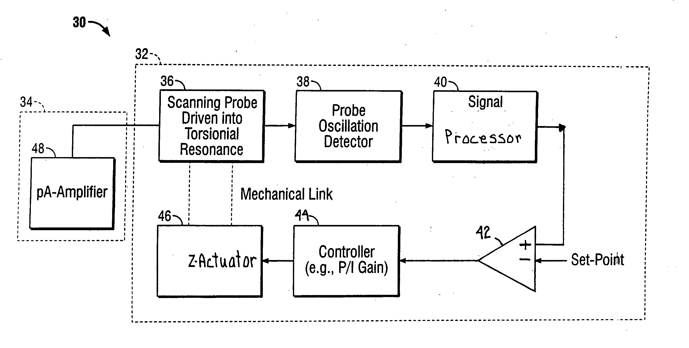
[0024] The preferred embodiments overcome the above-noted drawbacks by providing an atomic force microscopy apparatus and method that characterizes electrical properties of samples that consist of both conductive and non-conductive regions on the nanometer scale. Local electrical properties that can be measured by this technique include, but are not limited to: voltage, current, conductivity, resistivity, conduction current, tunneling current, dI / dV, dI / dz, surface potential, work function, capacitance, dC / dV, dC / dz, dielectric constant, dopant density, impedance, barrier height, and induced photovoltage. All of these are examples of localized electrical measurements that can be made by SPM. The system and method provide direct correlation of the location on a sample surface with its electrical properties by simultaneously mapping the topography and electrical current obtained when a bias is applied between the tip and the sample. In particular, the preferred embodiments enable nanometer scale measurement using ultra-low currents (60 fA to 120 pA) on very soft and delicate materials. In the preferred embodiments, TR mode is employed whereby the amplitude of the torsional resonance of the probe is used to control the probe so that it remains in close proximity to the sample surface, thus allowing precise measurement of the current between the tip and surface, at narrow (i.e., nanometer scale) tip-sample separations, during data acquisition. Alternatively, the probe may be oscillated at a lateral resonance.
[0035] In a still further embodiment, a method of operating a scanning probe microscope (SPM) includes measuring an electrical property of a sample with a probe. Notably, the sample can have an elastic modulus of generally less than 1 GPa. Even so, the measuring step is performed without plastic deformation of the sample.

Problems solved by technology

Notably, STM has a significant drawback.
In general, STM cannot be used to scan an insulating sample or a conductive with insulating surface layers such as oxide.
However, one drawback of this technique is that it uses the previously described contact mode of AFM operation, according to which a static vertical deflection force is utilized as the feedback signal to control the force, and thus the tip-surface distance, during scanning.
There are several problems associated with this.
First, the feedback can only maintain a constant force between the tip and the surface in the vertical direction.
When the tip scans across the surface, there is generally a large shear force present, and this high lateral force can easily damage both the tip and the sample.
This is a problem not only because of the high shear forces present in contact mode, but also because the measurement is useless if the tip and sample are not in contact.
This issue has seriously limited the use of AFM-based electrical characterization techniques on soft samples like conductive polymers.
Next, the sensitivity of contact mode is limited because feedback is based on a static signal, as opposed to a dynamic signal.
Static signals are more susceptible to thermal drift and charging, and thus sensitivity is compromised, as described in more detail below.
With no reference, static signal feedback is susceptible to thermal drift and electrostatic charging, creating significant problems given that these phenomena directly affect the sensitivity of the measurement, as understood in the art.
The Q factor also reduces the effective force applied by the tip to the sample.
Although this is a benefit for minimizing shear force, and thus sample damage, such minimal contact is a drawback in that the tip moves in and out of what is known as the “near field.” Because the tip of the probe must be in the near field to measure many electrical properties of the sample this often is a significant drawback with using oscillating mode to perform electrical measurements.
Overall, for these reasons, it is generally not possible to perform low current measurements on samples while operating in oscillation feedback mode.
In fact, the tip must be caused to penetrate a water layer that resides on the sample surface and then to push into the sample surface; otherwise, stable imaging cannot be achieved.
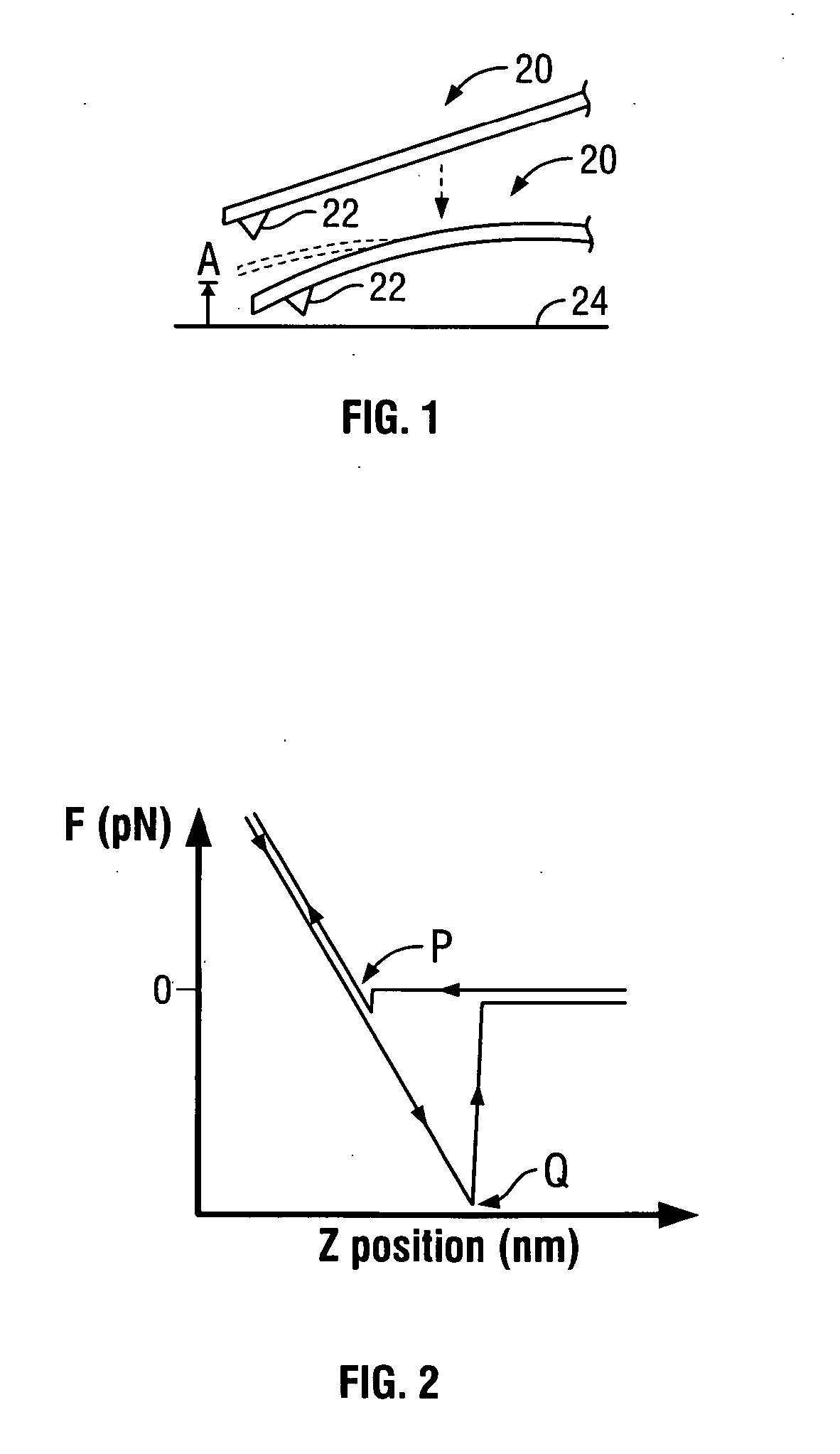
Contact mode cantilevers often suffer from a serious drawback in that they cannot be brought into close proximity to the sample surface without the tip snapping into contact with the surface.
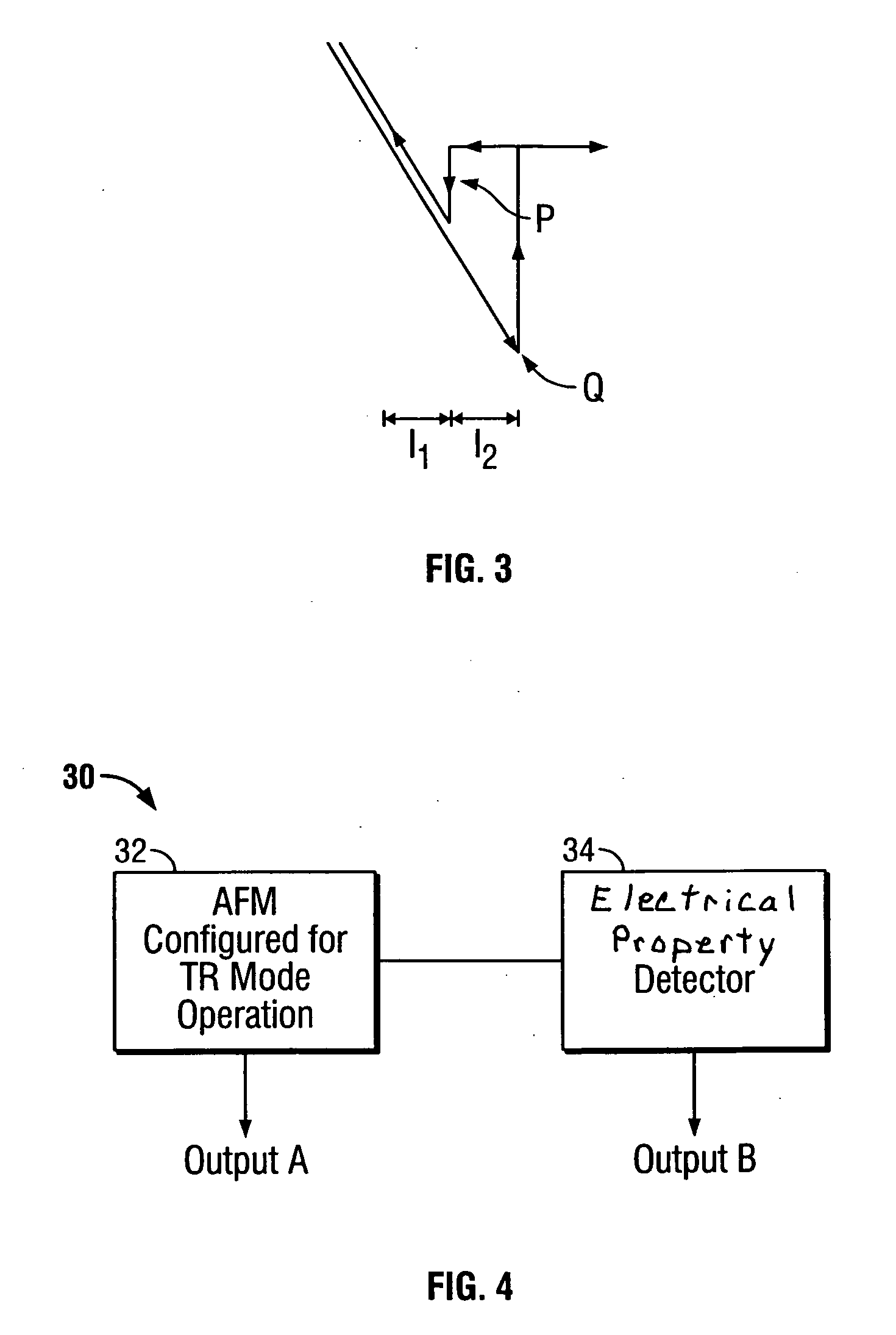
This is particularly a problem when performing force spectroscopy measurements, an illustration of which is discussed in connection with FIGS. 1-3.
As a result, deflection of the probe downwardly increases.
This action between the probe and the sample yields regions of instability in the tip-sample separation continuum where the AFM cannot “hold” the tip to perform a current measurement.

Method used


Image

  • Method and apparatus for measuring electrical properties in torsional resonance mode
  • Method and apparatus for measuring electrical properties in torsional resonance mode
  • Method and apparatus for measuring electrical properties in torsional resonance mode

Examples


Embodiment Construction

[0060] The preferred embodiments take advantage of the benefits provided by a new mode of AFM operation being developed known as torsional resonance mode (“TR mode), shown and described for instance in U.S. Ser. Nos. 10 / 189,108 and 10 / 937,597 to the present assignee. This technique includes driving a cantilever probe at its torsional resonance frequency and using the amplitude of oscillation at resonance for feedback control to keep the tip in proximity to the sample surface. As with other modes of AFM operation, these feedback signals are indicative of a characteristic of a sample, such as sample topography, and can be used to generate a map of the surface. In TR mode, the torsional resonance of the lever and changes thereto are measured by a four-quadrant photo detector. More particularly, the detector differentiates both vertical and horizontal components of probe motion, indicative of, cantilever flexural and torsional motion, respectively.

[0061] The damping of the RMS amplitud...


PUM


Abstract

The preferred embodiments are directed to a method and apparatus of operating a scanning probe microscope (SPM) including oscillating a probe of the SPM at a torsional resonance of the probe, and generally simultaneously measuring an electrical property, e.g., a current, capacitance, impedance, etc., between a probe of the SPM and a sample at a separation controlled by the torsional resonance mode. Preferably, the measuring step is performed while using torsional resonance feedback to maintain a set-point of SPM operation.

Description

CROSS REFERENCE TO RELATED APPLICATIONS [0001] This application is a non-provisional application claiming priority to provisional application No. 60 / 573,464, and is a continuation-in-part of U.S. patent application Ser. Nos. 10 / 189,108 filed on Jul. 2, 2002, and 10 / 937,597 filed on Sep. 9, 2004, the entirety of each of which is expressly incorporated by reference herein.BACKGROUND OF THE INVENTION [0002] 1. Field of the Invention [0003] The present invention is directed to operating a probe-based instrument in torsional resonance mode, and more particularly, a method and apparatus of performing electrical property measurements using torsional resonance feedback. [0004] 2. Description of Related Art [0005] Several probe-based instruments monitor the interaction between a cantilever-based probe and a sample to obtain information concerning one or more characteristics of the sample. Scanning probe microscopes (SPMs), such as the atomic force microscope (AFM), are devices which typicall...

Claims


Application Information

Patent Timeline
Patent Type & Authority Applications(United States)
IPC IPC(8): G01Q20/04G01Q30/06G01Q30/18G01Q60/30G01Q60/32G01Q60/34G01Q60/40G01Q60/48G01Q70/02G01R27/04G01R27/32
CPCB82Y35/00G01Q20/04G01Q30/06G01Q30/18G01Q10/065G01Q60/30G01Q60/32G01Q60/40G01Q60/48G01Q60/26
Inventor HUANG, LINSU, CHANMIN
Owner BRUKER NANO INC
Learn More