Data compression read mode for memory testing

a data compression and read mode technology, applied in the direction of error prevention, digital transmission, instruments, etc., can solve the problems of large quantities of flash memory consumed by digital cellular and wireless applications, device failure, and mismatch between any bit of any word of output data and input pattern, so as to improve the reliability of end-use, the time required for testing the ability of a memory device to accurately store data can be reduced

Inactive Publication Date: 2005-09-29
MICRON TECH INC
View PDF10 Cites 15 Cited by
  • Summary
  • Abstract
  • Description
  • Claims
  • Application Information

AI Technical Summary

Benefits of technology

[0011] Testing of memory devices is generally performed as part of a quality program to improve end-use reliability. The memory devices described herein are capable of a normal mode of operation and a test mode of operation. The test mode of operation includes a data compression test mode wherein reading one word of an output page provides as indication of the data values of the remaining words of the output page. In this manner, read time of a memory array having a repeating pattern can be reduced to a fraction of the time required to read every word of the array. Consequently, the time required for testing the ability of a memory device to accurately store data can be reduced.

Problems solved by technology

Digital cellular and wireless applications consume large quantities of flash memory and are continually pushing for lower voltages and higher densities.
A mismatch between any bit of any word of the output data and the input pattern is indicative of a device failure.
These tests, while valuable to verify device reliability, are time consuming and expensive.

Method used


Image

  • Data compression read mode for memory testing
  • Data compression read mode for memory testing
  • Data compression read mode for memory testing

Examples


Embodiment Construction

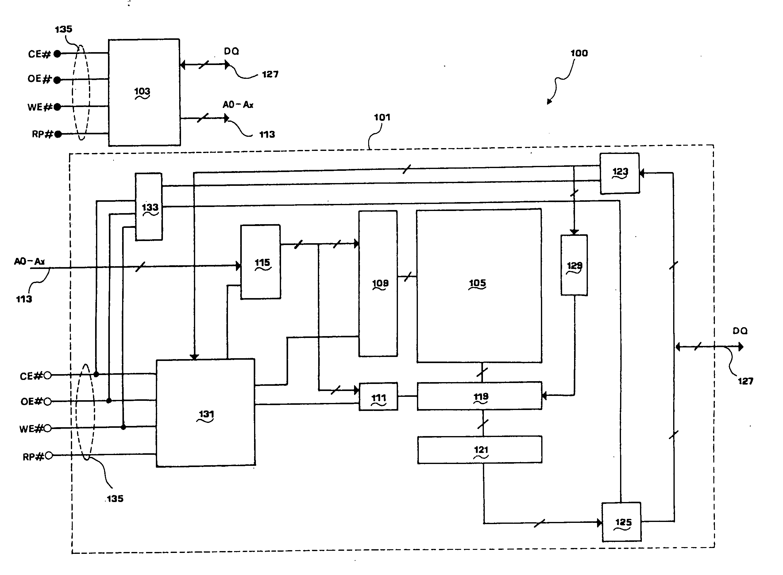
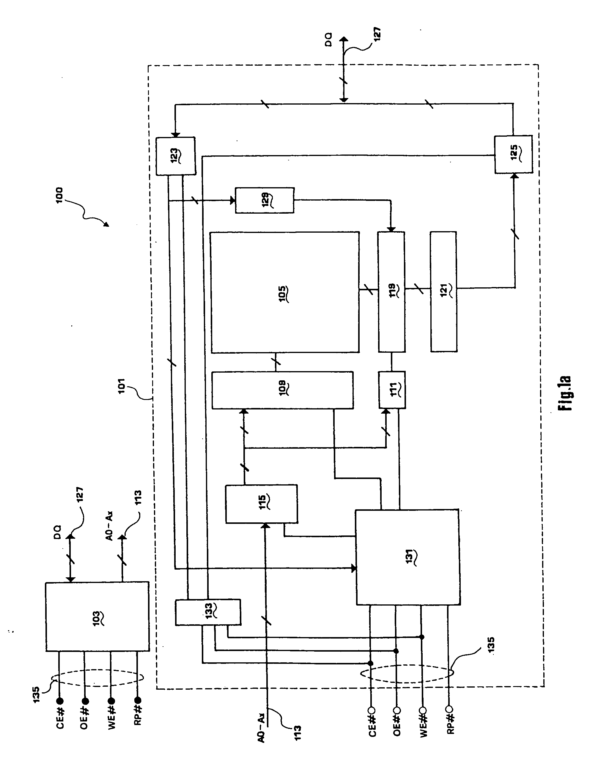
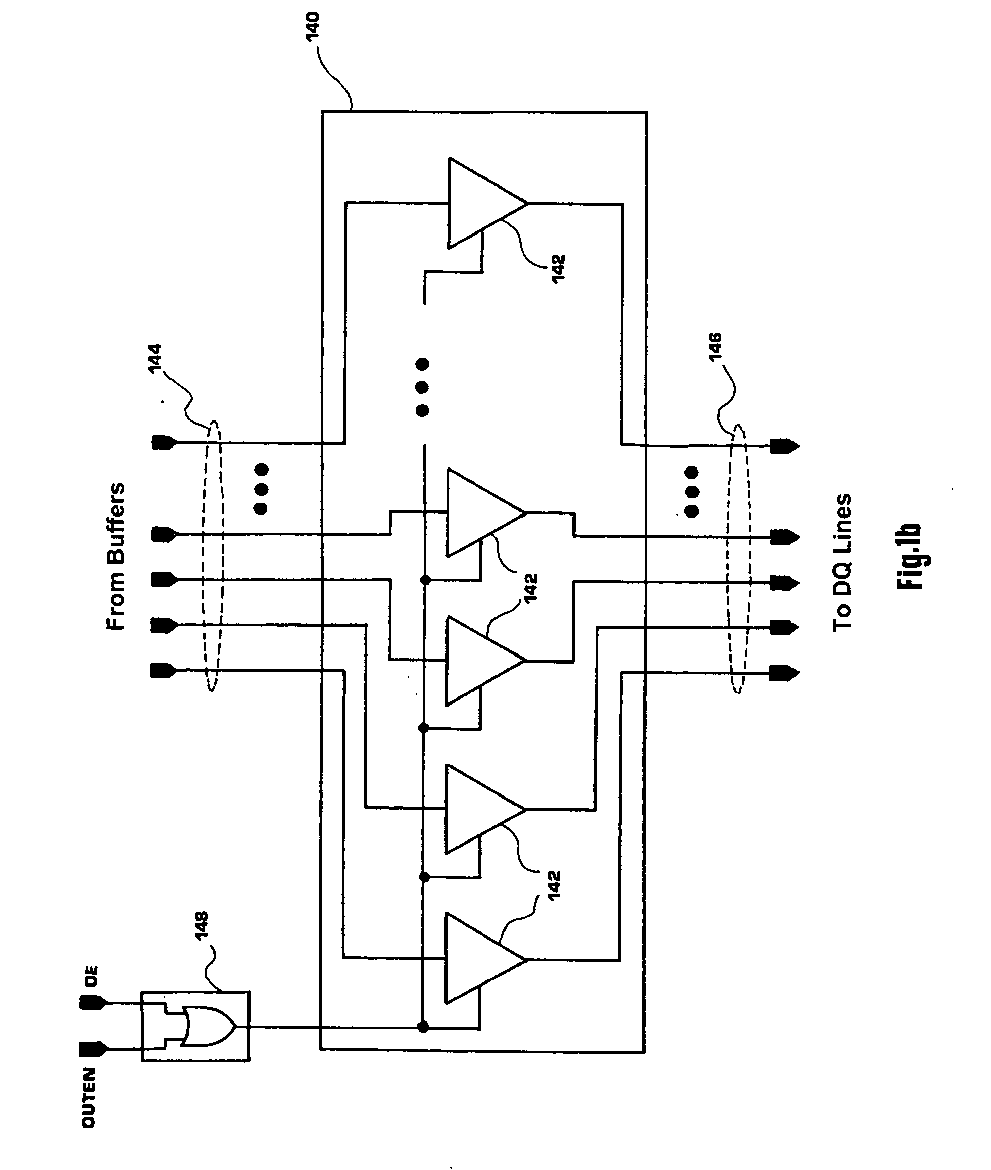
[0024] In the following detailed description of the present embodiments, reference is made to the accompanying drawings that form a part hereof, and in which is shown by way of illustration specific embodiments in which the invention may be practiced. These embodiments are described in sufficient detail to enable those skilled in the art to practice the invention, and it is to be understood that other embodiments may be utilized and that process, electrical or mechanical changes may be made without departing from the scope of the present invention. The terms wafer or substrate used in the following description include any base semiconductor structure. Examples include silicon-on-sapphire (SOS) technology, silicon-on-insulator (SOI) technology, thin film transistor (TFT) technology, doped and undoped semiconductors, epitaxial layers of a silicon supported by a base semiconductor structure, as well as other semiconductor structures well known to one skilled in the art. Furthermore, wh...


PUM


Abstract

Memory devices having a normal mode of operation and a test mode of operation are useful in quality programs. The test mode of operation includes a data compression test mode. In the data compression test mode, reading one word of an output page provides an indication of the data values of the remaining words of the output page. The time necessary to read and verify a repeating test pattern can be reduced as only one word of each output page need be read to determine the ability of the memory device to accurately write and store data values. The memory devices include data compression circuits to compare data values for each bit location of each word of the output page. Output is selectively disabled if a bit location for one word of the output page has a data value differing from any remaining word of the output page.

Description

RELATED APPLICATION [0001] This application is a continuation of U.S. patent application Ser. No. 09 / 943,642 (allowed), filed Aug. 30, 2001 and titled “DATA COMPRESSION READ MODE FOR MEMORY TESTING,” which is commonly assigned and incorporated by reference in its entirety herein, and which claims priority to Italian Patent Application RM2001A000104 filed Feb. 27, 2001.TECHNICAL FIELD OF THE INVENTION [0002] The present invention relates generally to semiconductor memory devices, and in particular, the present invention relates to test methods for semiconductor memory devices as well as circuits and apparatus for implementing such methods. BACKGROUND OF THE INVENTION [0003] Electronic information handling or computer systems, whether large machines, microcomputers or small and simple digital processing devices, require memory for storing data and program instructions. Various memory systems have been developed over the years to address the evolving needs of information handling syste...

Claims


Application Information

Patent Timeline
Patent Type & Authority Applications(United States)
IPC IPC(8): G11C29/40
CPCG11C29/40G11C29/1201
Inventor SANTIN, GIOVANNI
Owner MICRON TECH INC
Why Eureka
Try Eureka