Method for producing semiconductor device

Inactive Publication Date: 2005-09-29
ELPIDA MEMORY INC
View PDF6 Cites 9 Cited by
  • Summary
  • Abstract
  • Description
  • Claims
  • Application Information

AI Technical Summary

Benefits of technology

[0007] In such a process for reducing the stress on the silicon substrate by nitriding the oxide films on the inner walls, excessively high nitrogen concentrations in the resulting oxynitride films reduce the threshold voltages (Vth) of the

Problems solved by technology

In such a process for reducing the stress on the silicon substrate by nitriding the oxide films on the inner walls, excessively high nitrogen concentrations in the resulting oxynitride films reduce the threshold voltages (Vth) of the re

Method used


Image

  • Method for producing semiconductor device
  • Method for producing semiconductor device
  • Method for producing semiconductor device

Examples


embodiment 1

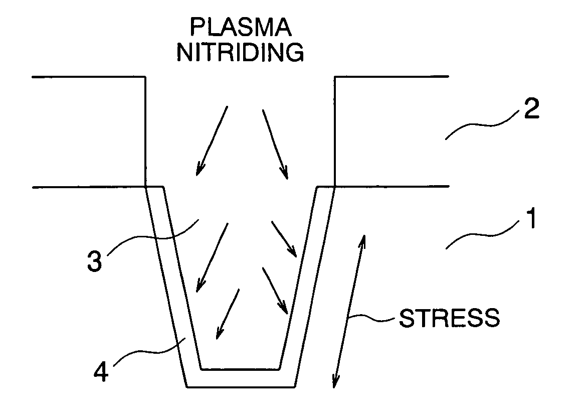
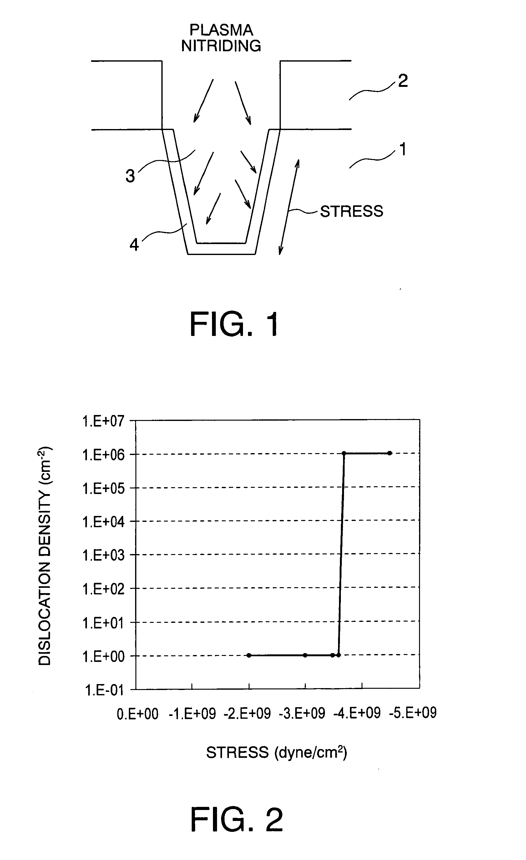
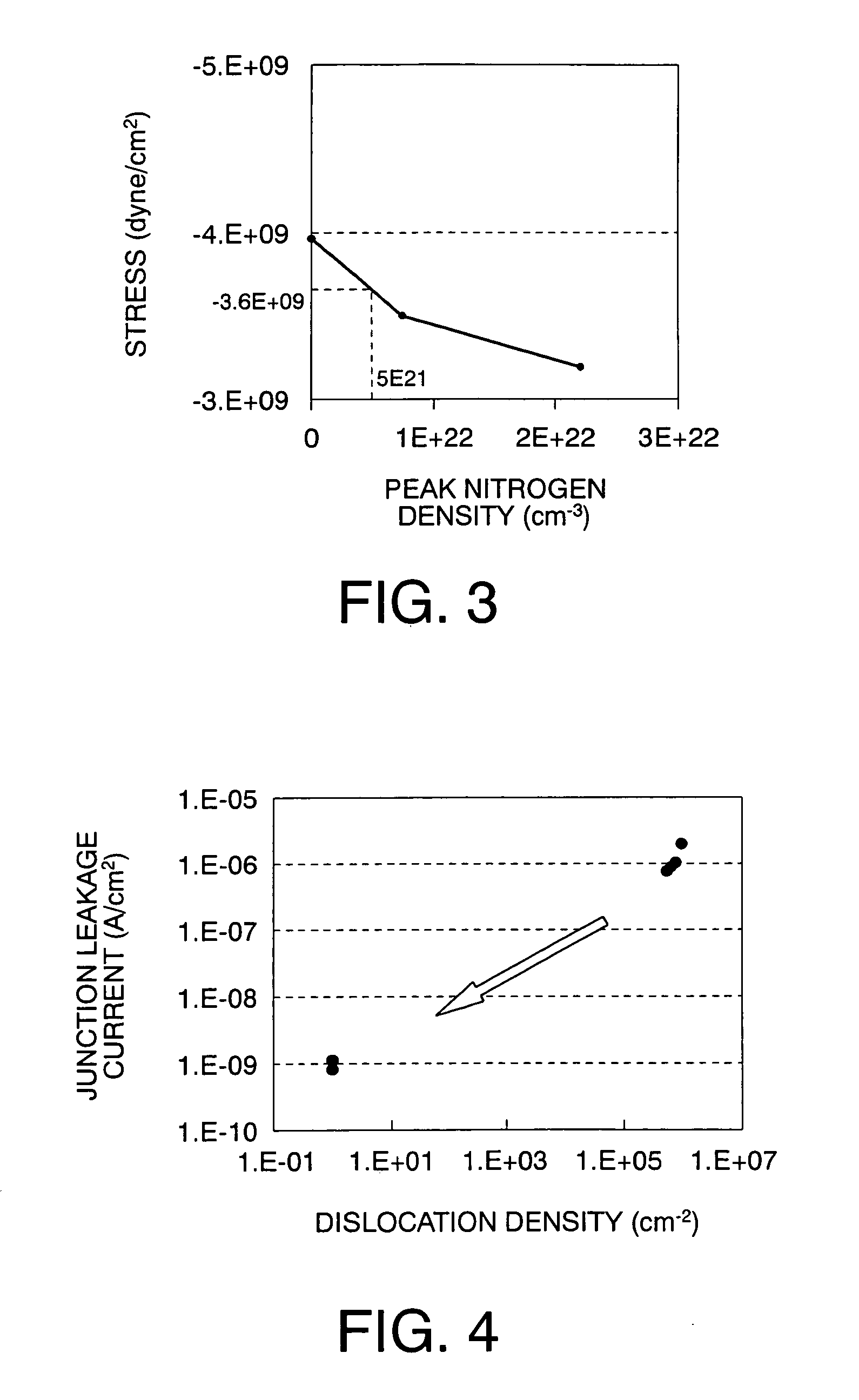
[0024] Embodiment 1 will now be described with reference to FIGS. 1 to 7. As shown in FIG. 1, a nitride film 2 is grown on a silicon substrate 1, and a trench 3 is formed by etching. The inner walls of the trench 3 are thermally oxidized to form inner-wall oxide films 4 each having a thickness of 5 to 20 nm. Then, the inner-wall oxide films 4 are partially nitrided by plasma to produce oxynitride films. A plasma oxide film is formed in the trench by plasma oxidation so as to be embedded in the entire trench. As a result, an isolation region for isolating elements from each other is produced. The peak nitrogen concentration in each oxynitride film is controlled to be optimized. By optimizing the peak nitrogen concentration, it is possible to reduce a stress and thus to suppress the occurrence of the dislocation defect in the silicon substrate. It is also possible to suppress a threshold voltage shift due to the positive charge of nitrogen.

[0025] Nitrogen in the oxynitride film funct...

embodiment 2

[0038] Embodiment 2 will be described below with reference to FIGS. 8 to 11. In Embodiment 1, each of the inner-wall oxide films 4 shown in FIG. 1 is nitrided by plasma to produce an oxynitride film. However, in this Embodiment 2, each of the inner-wall oxide films 4 is heat-treated in a nitrogen-containing atmosphere to produce an oxynitride film.

[0039] Each oxide film having a thickness of 5 to 20 nm is heat-treated in an atmosphere containing, for example, NH3, NO, or N2O to produce an oxynitride film. Heat-treating for nitriding the oxide film provides a broad distribution of the nitrogen concentration compared with plasma nitriding. The nitrogen concentration is increased at a Si—SiO2 interface. Thus, the peak nitrogen concentration is reduced and is in the range of 3E21 to 1E22 (cm−3). This concentration is achieved by heat-treating in NH3 at 950° C. for 60 seconds. In NO atmosphere, the concentration is achieved by heat-treating at 950° C. for 40 seconds under a pressure of ...


PUM


Abstract

With respect to nitriding of an oxide film on an inner wall of a trench, a method for producing a semiconductor device is provided, the method preventing the characteristic deterioration of the semiconductor device by controlling and optimizing peak nitrogen concentration in an oxide film to reduce the stress and to suppress the threshold voltage shift due to the positive charge of nitrogen.

Description

[0001] This application claims priority to prior Japanese patent application JP 2004-89887, the disclosure of which is incorporated herein by reference. BACKGROUND OF THE INVENTION [0002] 1. Field of the Invention [0003] The present invention relates to a method for producing an isolation region for isolating elements from each other in a semiconductor device. [0004] 2. Description of the Related Art [0005] Shallow trench isolation (STI) has been known as a process for isolating elements from each other in a semiconductor device. As shown in FIG. 12, the STI is performed as follows: A nitride film 2 is grown on a silicon substrate 1. A trench 3 is formed by etching. The inner walls of the trench 3 are thermally oxidized to form inner-wall oxide films 4. Another oxide film is formed in the trench by plasma oxidation so as to be embedded in the entire trench. In this way, the isolation region is produced. [0006] In this process, the oxide films 4 each having a thermal expansion coeffi...

Claims


Application Information

Patent Timeline
IPC IPC(8): H01L21/762H01L21/8234H01L21/76H01L21/8242H01L27/108
CPCH01L21/823481H01L21/76224
Inventor OHASHI, TAKUOKUBOTA, TAISHISAKURAI, SUSUMUKANDA, TAKAYUKI
Owner ELPIDA MEMORY INC
Why Eureka
Try Eureka