Semiconductor device and method of manufacturing the same

a technology of semiconductor devices and semiconductor devices, applied in semiconductor devices, semiconductor/solid-state device details, electrical apparatus, etc., can solve the problems of insufficient control of the growth mode of carbon nanotubes, the disadvantage of semiconductor devices in terms of production cost and reliability, and the remaining catalyst metal such as fe or co may be a problem in some semiconductor devices

Active Publication Date: 2005-09-29
FUJITSU LTD
View PDF5 Cites 136 Cited by
  • Summary
  • Abstract
  • Description
  • Claims
  • Application Information

AI Technical Summary

Benefits of technology

[0012] Accordingly, it is a general object of the present invention to provide a semiconductor device and a method of manufacturing the same in which the above-described disadvantages are eliminated.

Problems solved by technology

In the case of selectively forming carbon nanotubes, a process of patterning a catalyst metal layer is additionally required, which is a disadvantage in terms of the production cost and the reliability of a semiconductor device.
The remaining of catalyst metal such as Fe or Co may be a problem in some semiconductor devices.
However, according to such methods, the growth mode of the carbon nanotube cannot be controlled sufficiently.
This results in a problem in that the above-described electric characteristics of the carbon nanotube cannot be fully realized in the case of employing carbon nanotubes as interconnect material in the interconnection part and the vertical interconnection part of a semiconductor device.
Further, if complete removal of catalyst metal is required, there is a problem in that the catalyst layer remains at the root of any carbon nanotube grown in a root-growth mode, thus resulting in insufficient removal of the catalyst metal.
Further, in the case of employing the carbon nanotube in a vertical interconnection part, such as a via, of a semiconductor device, the catalyst metal layer and Al or Cu used in an interconnection part connected to the vertical interconnection part are subject to interdiffusion, thus resulting in the problem of a decline in the catalytic function.
Further, when an interlayer insulating film is formed on the catalyst metal layer, a plasma or ions collide or come into contact with the surface of the catalyst metal layer, thus causing physical damage thereto.
This also results in the problem of a decline in the catalytic function.

Method used


Image

  • Semiconductor device and method of manufacturing the same
  • Semiconductor device and method of manufacturing the same
  • Semiconductor device and method of manufacturing the same

Examples


first embodiment

[0051] [First Embodiment]

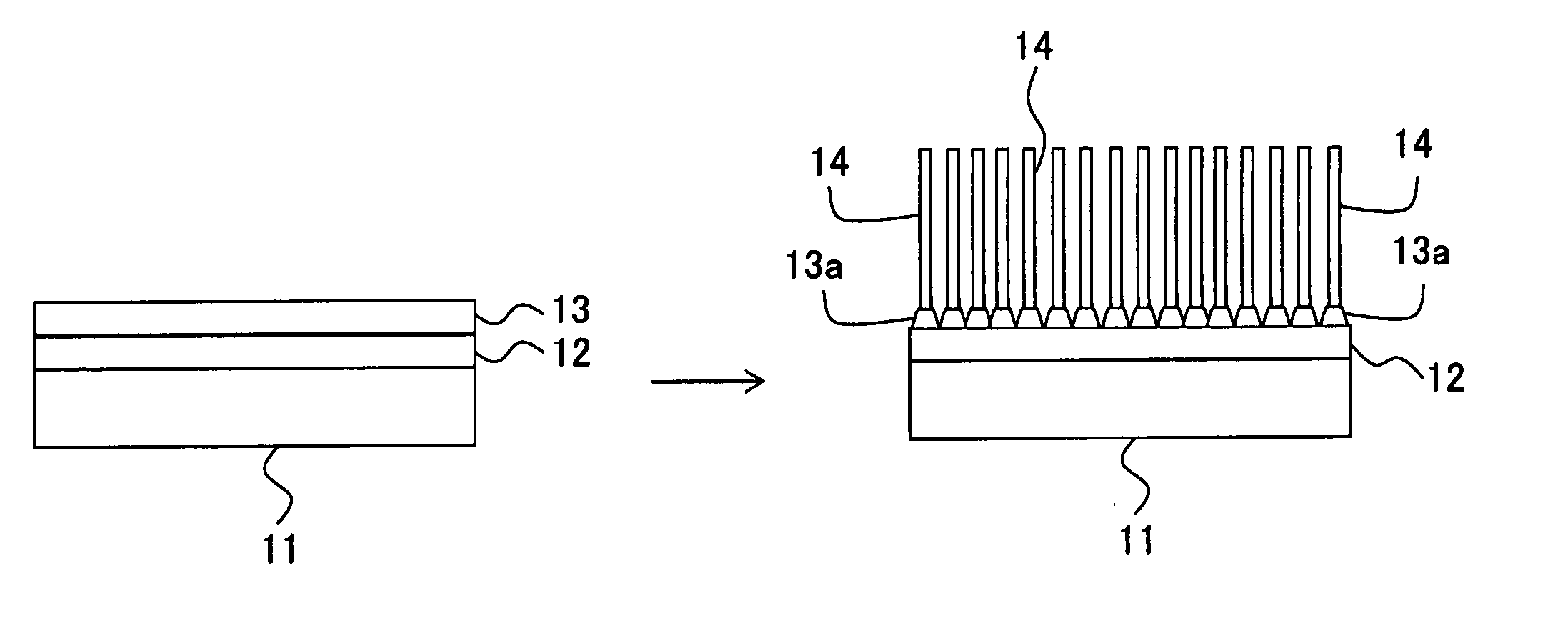
[0052] In this embodiment, a semiconductor device having contacts formed of quality carbon nanotubes that are selectively formed at low temperature is disclosed.

[0053]FIG. 3 is a sectional view of part of a semiconductor device 20 according to the first embodiment of the present invention.

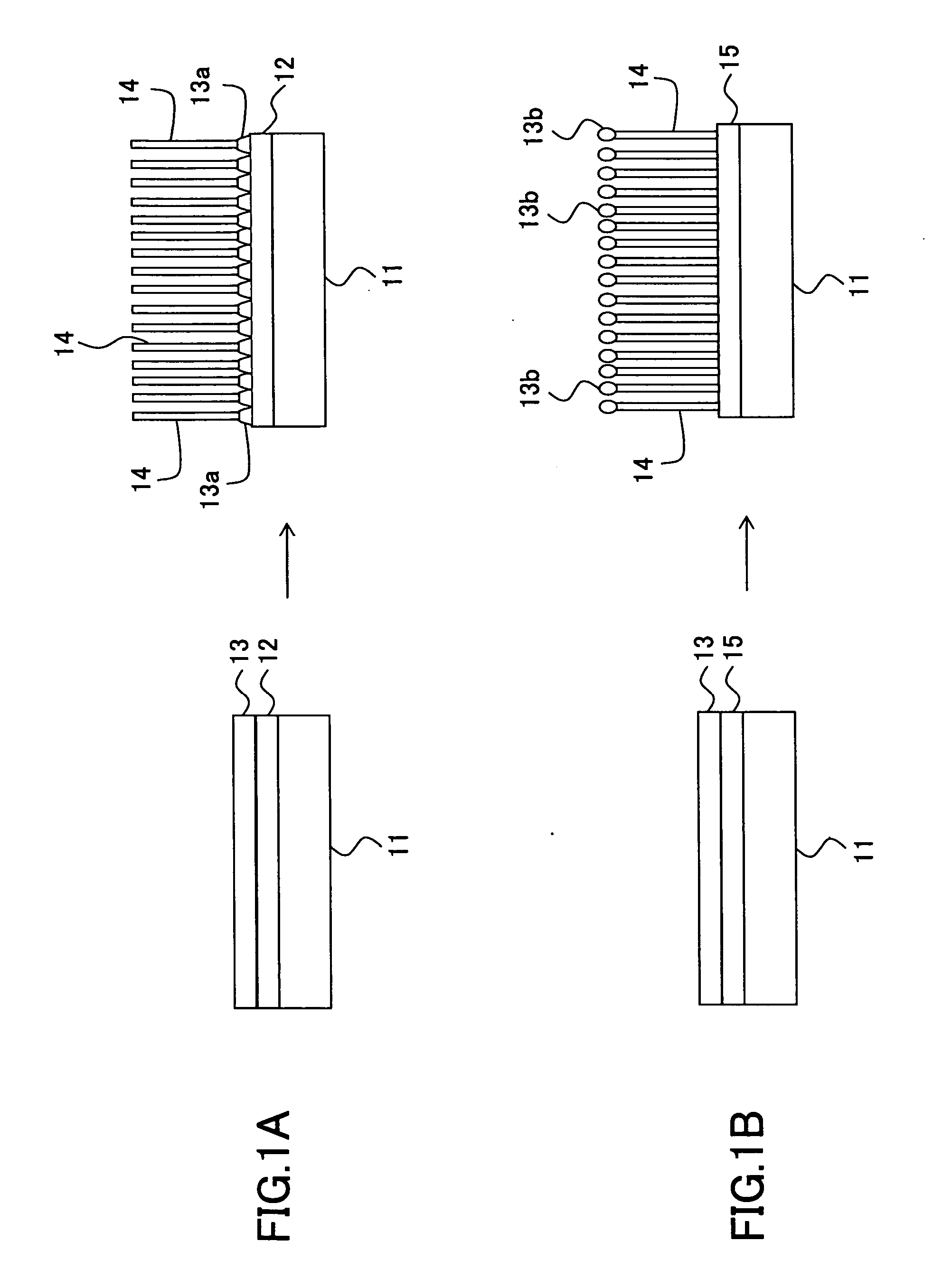
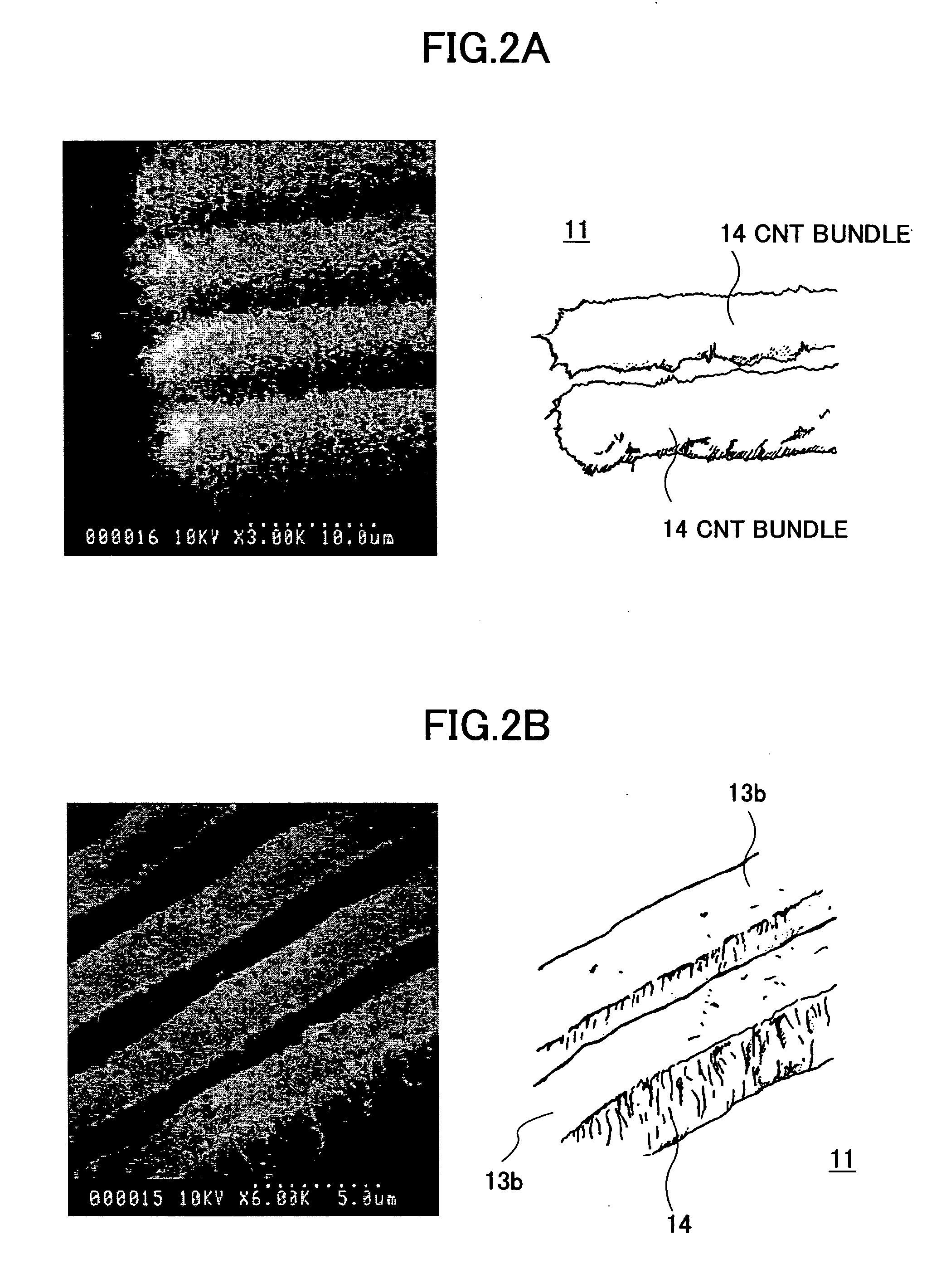
[0054] Referring to FIG. 3, the semiconductor device 20 includes a substrate 21 such as a silicon substrate, a contact 29 formed on the substrate 21, an alloy layer 25 and an interlayer insulating layer 28 that are formed in the region other than the contact 29, and an interconnection part 30 that is formed on the interlayer insulating film 28 so as to be in contact with the surface of the contact 29. The contact 29 is composed of a growth mode control layer 22, a particulate catalyst layer 23a, and carbon nanotubes (CNTs) 26 grown upward from the particulate catalyst layer 23a, which serves as a nucleus of growth. In the semiconductor device 20, an active layer (not grap...

second embodiment

[0077] [Second Embodiment]

[0078] In this embodiment, a semiconductor device with a contact formed of quality carbon nanotubes of high density is disclosed. According to the second embodiment, a protection film is formed on the surface of a catalyst layer, and the protection film is removed immediately before causing the carbon nanotubes to grow so as to prevent a decline in the catalytic function of the catalyst layer during a manufacturing process.

[0079]FIG. 6 is a sectional view of part of a semiconductor device 40 according to the second embodiment of the present invention. In FIG. 6, the same elements as those described above are referred to by the same numerals, and a description thereof is omitted.

[0080] Referring to FIG. 6, the semiconductor device 40 includes the substrate 21 such as a silicon substrate, the growth mode control layer 22 formed on the substrate 21, a contact 43 formed on the growth mode control layer 22, and the interconnection part 30 formed on the contact...

third embodiment

[0101] [Third Embodiment]

[0102] In this embodiment, a semiconductor device including a via composed of carbon nanotubes formed selectively on an interconnection part is disclosed.

[0103]FIG. 9 is a sectional view of part of a semiconductor device 60 according to the third embodiment of the present invention. In FIG. 9, the same elements as those described above are referred to by the same numerals, and a description thereof is omitted.

[0104] Referring to FIG. 9, the semiconductor device 60 includes a first interlayer insulating film 28-1, a first interconnection part 30-1 formed on the first interlayer insulating film 28-1, a growth mode control layer 61 formed on the first interconnection part 30-1, a via 62 formed selectively on the growth mode control layer 61 so as to be electrically connected to the first interconnection part 30-1, a second interlayer insulating film 28-2 formed in the region other than the region of the via 62, and a second interconnection part 30-2 formed on...


PUM

PropertyMeasurementUnit
temperatureaaaaaaaaaa
thicknessaaaaaaaaaa
resistanceaaaaaaaaaa

Abstract

A method of manufacturing a semiconductor device having an interconnection part formed of multiple carbon nanotubes is disclosed. The method includes the steps of (a) forming a growth mode control layer controlling the growth mode of the carbon nanotubes, (b) forming a catalyst layer on the growth mode control layer, and (c) causing the carbon nanotubes to grow by heating the catalyst layer by thermal CVD so that the carbon nanotubes serve as the interconnection part. The growth mode control layer is formed by sputtering or vacuum deposition in an atmospheric gas, using a metal selected from a group of Ti, Mo, V, Nb, and W. The growth mode is controlled in accordance with a predetermined concentration of oxygen gas of the atmospheric gas.

Description

CROSS-REFERENCE TO RELATED APPLICATION [0001] The present application is based on Japanese Priority Patent Application No. 2004-093075, filed on Mar. 26, 2004, the entire contents of which are hereby incorporated by reference. BACKGROUND OF THE INVENTION [0002] 1. Field of the Invention [0003] The present invention relates generally to semiconductor devices and methods of manufacturing the same, and more particularly to a semiconductor device including carbon nanotubes in an interconnection layer and through electrodes and a method of manufacturing such a semiconductor device. [0004] 2. Description of the Related Art [0005] Application of carbon nanotubes to the interconnects of a large scale integrated circuit (LSI) is taken as an example of their application to electronics. Carbon nanotubes range from a few to tens of nm in diameter, and are as long as a few nanometers in length. Because of its one-dimensional electronic properties due to this shape anisotropy, the carbon nanotube...

Claims


Application Information

Patent Timeline
Patent Type & Authority Applications(United States)
IPC IPC(8): H01L21/28H01L21/285H01L21/3205H01L21/4763H01L21/768H01L23/532
CPCB82Y10/00H01L21/28562H01L21/76879H01L21/76885H01L21/76898H01L23/481Y10S257/914H01L23/53276H01L2221/1094H01L2924/0002H01L2924/00
Inventor HORIBE, MASAHIROKAWABATA, AKIONIHEI, MIZUHISA
Owner FUJITSU LTD
Why Eureka
Try Eureka