Semiconductor device and manufacturing method for the same

a technology of semiconductor devices and manufacturing methods, applied in semiconductor devices, semiconductor/solid-state device details, capacitors, etc., can solve the problem of limiting the selection of materials of the lower electrode, and achieve the effect of high-reliability mim structur

Active Publication Date: 2005-10-06
RENESAS ELECTRONICS CORP
View PDF12 Cites 27 Cited by
  • Summary
  • Abstract
  • Description
  • Claims
  • Application Information

AI Technical Summary

Benefits of technology

[0010] An object of the present invention is to provide a semiconductor device including a capacitive element having a highly reliable MIM structure.

Problems solved by technology

In the prior art, the lower electrode is provided in contact with the lower interconnection, and the lower electrode is formed above the lower copper interconnection or barrier metal provided on the lower copper interconnection, so that there is a definite limitation in selection of the material of the lower electrode.

Method used


Image

  • Semiconductor device and manufacturing method for the same
  • Semiconductor device and manufacturing method for the same
  • Semiconductor device and manufacturing method for the same

Examples


first embodiment

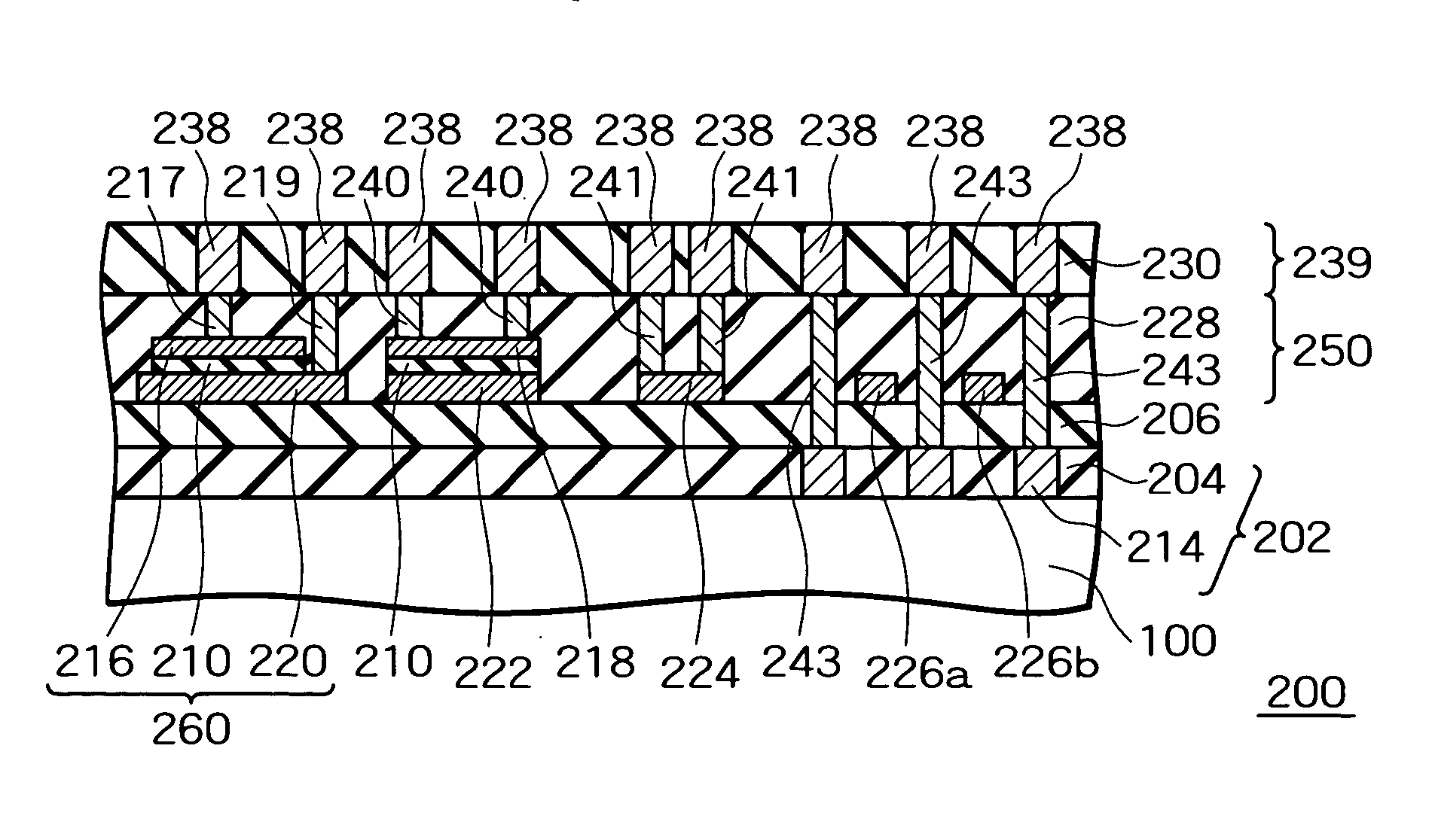
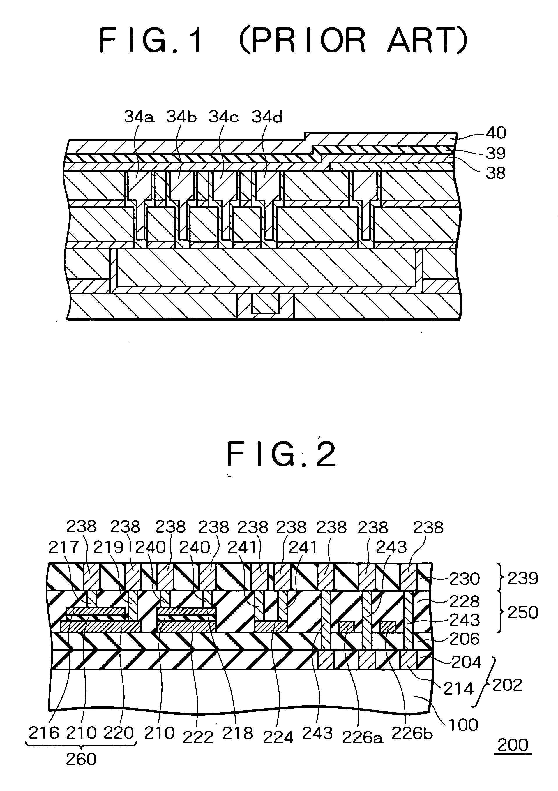
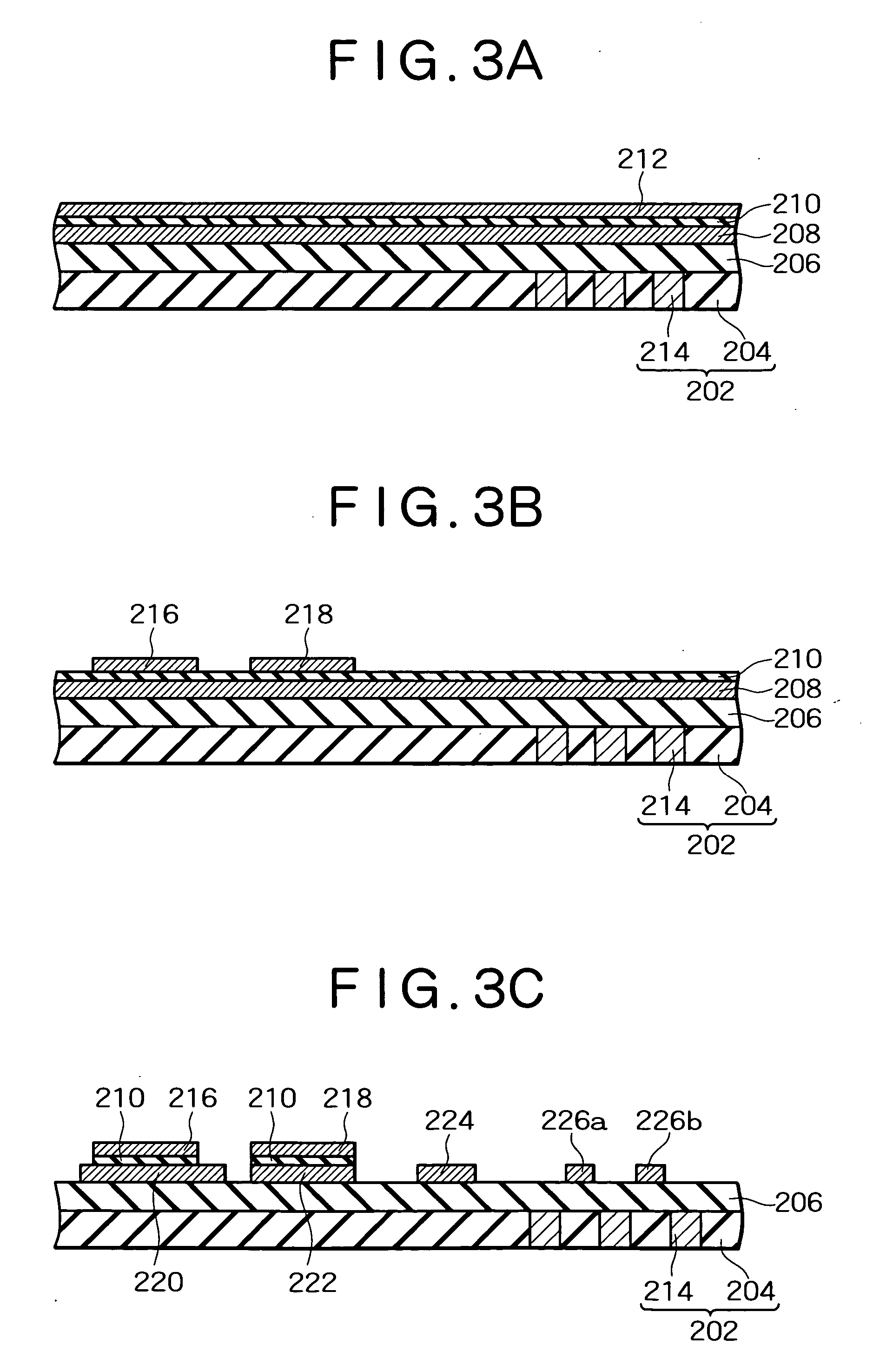
[0038] A semiconductor device according to the first embodiment has a structure in which passive elements including an MIM capacitive element and a resistive element are provided in a logic circuit element including a multilayer copper interconnection. FIG. 2 is a sectional view showing the construction of a semiconductor device 200 according to this embodiment. The semiconductor device 200 has a structure in which a silicon substrate 100, a first copper interconnection layer 202, an interlayer insulation film 206, a passive element layer 250, and a second copper wiring layer 239 are layered in this order. The first copper interconnection layer 202 and the second copper interconnection layer 239 are copper interconnections in a multilayer interconnection including, for example, six to ten layers. The first copper interconnection layer 202 corresponds to a copper interconnection layer of the first layer immediately above a layer in which a transistor is formed. The second copper inte...

second embodiment

[0075] Next, a second embodiment of the present invention is described. A semiconductor device according to this embodiment is provided with inductive element in the same layer including MIM capacitive element. FIG. 4 is a sectional view showing the construction of the semiconductor device 300 of this embodiment, and FIG. 5 shows the structure of the inductive element 270 of FIG. 4 viewed from above. In FIG. 5, the inductive element 270 includes a first conductor 242, a second conductor 244, a third conductor 246, a fourth conductor 248, via plugs 245, and upper copper interconnections 238, the first conductor 242, the second conductor 244, the third conductor 246, and the fourth conductor 248 being provided at the same level as the lower electrode 220. Herein, connection is made between the end of the first conductor 242 and the via plugs 245, between the end of the second conductor 244 and the via plug 245, between the end of the third conductor 246 and the via plug 245, and betwe...


PUM


Abstract

A lower interconnection is provided on a semiconductor substrate. A MIM capacitive element is provided on a first interlayer insulation film in which the lower interconnection is buried, and includes a lower electrode, an upper electrode, and a dielectric film sandwiched therebetween. An upper interconnection is provided on a second interlayer insulation film in which the MIM capacitive element is buried. A contact electrically connects the lower electrode and the upper interconnection. The lower electrode is mainly formed of Al, so that they are lower in electrical resistance than barrier metal, and also low in stress value. Therefore, it becomes possible to widen the area of the lower electrode for electrically connecting the contact while restraining their influences on charge accumulation and close contact between the lower electrode and the insulation film. In addition, since the electrical resistance is lowered, the thickness of the lower electrode can be increased. Accordingly, the MIM capacitive element with a large capacitance can be manufactured with a high yield.

Description

BACKGROUND OF THE INVENTION [0001] 1. Technical Field of the Invention [0002] The present invention relates to a semiconductor device including a capacitive element with an MIM structure. [0003] 2. Description of the Related Art [0004] An RF (radio-frequency) analog device comprises active elements for handling high-frequency signals and passive elements such as resistive elements and capacitive elements. In RF analog devices, reduction of parasitic resistances and parasitic capacitances is demanded in view of improvement in high-speed operability and reduction in power consumption. Therefore, in capacitive elements, an MIM (Metal-Insulator-Metal) capacitive element is widely used in which parasitic resistances and parasitic capacitances are remarkably smaller than those of conventional MOS capacitive elements. [0005] On the other hand, a structure in which such an RF analog device is installed inside a logic device and formed into one chip has also been developed. In order to reali...

Claims


Application Information

Patent Timeline
Patent Type & Authority Applications(United States)
IPC IPC(8): H01L27/04H01L21/02H01L21/822H01L23/522H01L27/01H01L27/108
CPCH01L23/5223H01L27/016Y10S257/924Y10S257/923H01L28/55H01L2924/0002H01L2924/00
Inventor KIKUTA, KUNIKONAKAYAMA, MAKOTO
Owner RENESAS ELECTRONICS CORP
Why Eureka
Try Eureka