Thin film magnetic memory device suitable for drive by battery

a magnetic memory and thin film technology, applied in the direction of information storage, static storage, digital storage, etc., can solve the problems of limited electric power supply from a battery, accelerate battery exhaustion, and difficult to ensure the electric power capacity of the power supply in an application, so as to reduce the number of switching elements to be arranged, the effect of improving the quality of the magnetic memory devi

Inactive Publication Date: 2005-10-06
RENESAS ELECTRONICS CORP
View PDF3 Cites 7 Cited by
  • Summary
  • Abstract
  • Description
  • Claims
  • Application Information

AI Technical Summary

Benefits of technology

[0016] Therefore, in the thin film magnetic memory device according to the present invention, charges stored in the first write current line prior to a first data write current supply period are used to feed the first data write current. Accordingly, concentration of the load current supplied from the power supply such as a battery to the thin film magnetic memory device during the data write current period and a resultant short-period, large-current waveform causing considerable battery exhaustion is avoided, and the load current supplied from the power supply can exhibit an improved, gentle waveform. Consequently, the period for electric power supply from the power supply (battery) can be extended, and a time period for which equipment incorporating the thin film magnetic memory device (MRAM device) can be driven can be extended.
[0017] In particular, the second switching element is provided so that charging of the first write current line and supply of the first data write current can be carried out in different periods. Therefore, the load current supplied from the power supply can exhibit a further improved, gentle waveform.
[0018] In addition, one side of the write current line is connected to the write node set to a voltage in accordance with the write data, while the other side thereof is connected to a voltage different from the voltage set at the write node by means of a plurality of write switching elements that are selectively turned on. In this manner, a data write current in a direction in accordance with the write data can flow on the write current line. Therefore, as compared with a configuration in which a plurality of write switches are provided on each side of the write current line, the number of switching elements to be arranged can be reduced. Moreover, as compared with a configuration in which complementary data buses are arranged on opposing sides of the write current line respectively, a path for the data write current can be shortened and a parasitic resistance on that path can be suppressed. In the thin film magnetic memory device, reduction in the circuit area and facilitated manner of ensuring the magnitude of the data write current can thus be realized in a balanced manner.
[0019] Alternatively, a plurality of write current lines may share a write driver on one end side of the write current line, and a write driver on the other end side may be arranged for each current write line. With such a configuration as well, a data write current in a direction in accordance with the write data can flow on the write current line. Therefore, while avoiding an extended length of a path for the data write current, the number of write drivers to be arranged can be reduced. In this manner, reduction in the circuit area and facilitated manner of ensuring the magnitude of the data write current can both be realized in the thin film magnetic memory device.

Problems solved by technology

With regard to portable use, as it is difficult to constantly supply electric power from an outside source, limited electric power supply from a battery or the like is performed.
In general, such a load current pattern accelerates battery exhaustion.
In addition, it is difficult to ensure electric power capacity of the power supply in an application such as an IC card or the like.
Therefore, it is necessary to ensure a sufficient data write current level within the MRAM device serving as a load under such a condition that a peak value of the load current supplied by the power supply is restricted.

Method used


Image

  • Thin film magnetic memory device suitable for drive by battery
  • Thin film magnetic memory device suitable for drive by battery
  • Thin film magnetic memory device suitable for drive by battery

Examples


first embodiment

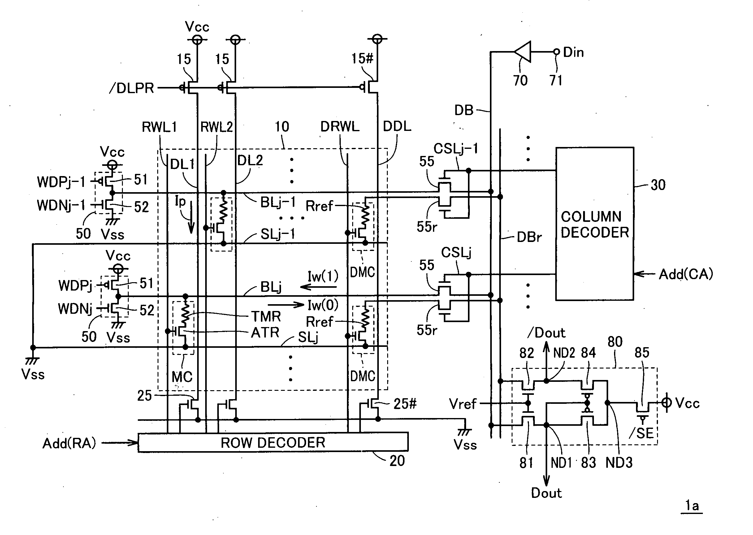
[0069]FIG. 1 is a schematic block diagram showing an overall configuration of an MRAM device 1a according to a first embodiment of the present invention.

[0070] Referring to FIG. 1, the MRAM device carries out random access in response to an external control signal (not shown) and an address signal Add, and receives input of write data Din and supplies output of read data Dout. An internal operation of an MRAM device 1 represented by a data read operation and a data write operation is carried out by a not-shown control circuit in response to the control signal. The internal operation is performed, for example, at a timing in synchronization with an external clock signal (not shown). Alternatively, an operation timing may be determined within the MRAM without receiving an external clock signal.

[0071] MRAM device 1a includes a memory cell array 10, a row decoder 20, a column decoder 30, a write buffer 70, a data read amplifier 80, and a data bus DB and a reference data bus DBr.

[0072...

second embodiment

[0210] As described in the first embodiment, in the MRAM device according to the present invention, sufficient charge capacitance of digit line DL and bit line BL should be obtained in order to ensure an amount of data write current and the current supply period. In a second embodiment, a configuration to obtain the charge capacitance using a hierarchically higher write line provided hierarchically with respect to digit line DL and bit line BL will be described.

[0211]FIG. 16 is a schematic block diagram showing an overall configuration of an MRAM device 1b according to the second embodiment of the present invention.

[0212] When FIG. 16 is compared with FIG. 1, in MRAM device 1b according to the second embodiment, each digit line DL is connected to a main digit line MDL through transistor switch 15. Main digit line MDL represents a “hierarchically higher write line” commonly and hierarchically provided with respect to digit lines DL. A voltage signal φ(DL) is applied to main digit l...

third embodiment

[0264]FIG. 26 is a schematic block diagram showing an overall configuration of an MRAM device 1c according to a third embodiment of the present invention.

[0265] Referring to FIG. 26, MRAM device 1c according to the third embodiment is different in part from MRAM device 1b according to the second embodiment shown in FIG. 16 in the configuration for supplying bit line BL with the data write current. Specifically, a data bus / WDB and a column selection switch 56 are newly provided, instead of write driver 50 provided corresponding to one end of each bit line BL.

[0266] Write data bus / WDB is driven to the data voltage in accordance with inverted data / Din of write data Din by a write buffer 70#. That is, write buffers 70 and 70# drive write data buses WDB and / WDB with voltages complementary to each other, in accordance with write data Din. Specifically, when Din=“H level”, write data bus / WDB is driven to power supply voltage Vcc, while write data bus / WDB is driven to ground voltage...


PUM


Abstract

After a digit line is charged to a power supply voltage by turn-on of a first switching element, the first switching element is turned off and a second switching element is turned on, whereby the digit line is connected to a ground voltage. Similarly, in order to feed data write current, a bit line is charged to a data voltage in accordance with write data through a third switching element. Then, the bit line is connected to a voltage different from the data voltage by a fourth switching element while the third switching element is turned off. Therefore, a load current from a power supply to an MRAM device is supplied during charging of a digit line capacitance and a bit line capacitance, without being consumed when the data write current flows. Consequently, a peak of the load current supplied from the power supply is suppressed.

Description

BACKGROUND OF THE INVENTION [0001] 1. Field of the Invention [0002] The present invention relates to a thin film magnetic memory device, and more particularly, to a thin film magnetic memory device suitable for drive by a battery. [0003] 2. Description of the Background Art [0004] Recently, a magnetic random access memory device (MRAM device) has attracted attention as a high-speed and highly integrated non-volatile memory. The MRAM device represents a memory device using a plurality of thin film magnetic elements formed on a semiconductor integrated circuit as a memory cell permitting random access thereto. [0005] Particularly, it has been disclosed that a performance of the MRAM device is enhanced by employing a memory cell constituted of thin film magnetic elements utilizing magnetic tunnel junction (MTJ) (hereinafter, also referred to as an “MTJ memory cell”). The MTJ memory cell stores data, by being magnetized in a direction in accordance with write data by a magnetic field pr...

Claims


Application Information

Patent Timeline
Patent Type & Authority Applications(United States)
IPC IPC(8): G11C11/15G11C11/14
CPCG11C11/16
Inventor HIDAKA, HIDETO
Owner RENESAS ELECTRONICS CORP
Why Eureka
Try Eureka