

Pattern inspection method, pattern inspection system and pattern inspection program of photomask
a technology of pattern inspection and inspection method, which is applied in the direction of originals for photomechanical treatment, image enhancement, instruments, etc., can solve the problems of inability to accurately determine the finer pattern, inability to correct the defect location of the reticle pattern with ease, and inability to accurately determine the fine pattern. , to achieve the effect of reducing the pattern inspection time of the photomask, reducing the difficulty of inspection, and easy identification
- Summary
- Abstract
- Description
- Claims
- Application Information
AI Technical Summary
Benefits of technology
Problems solved by technology
Method used
Image

Examples
first embodiment
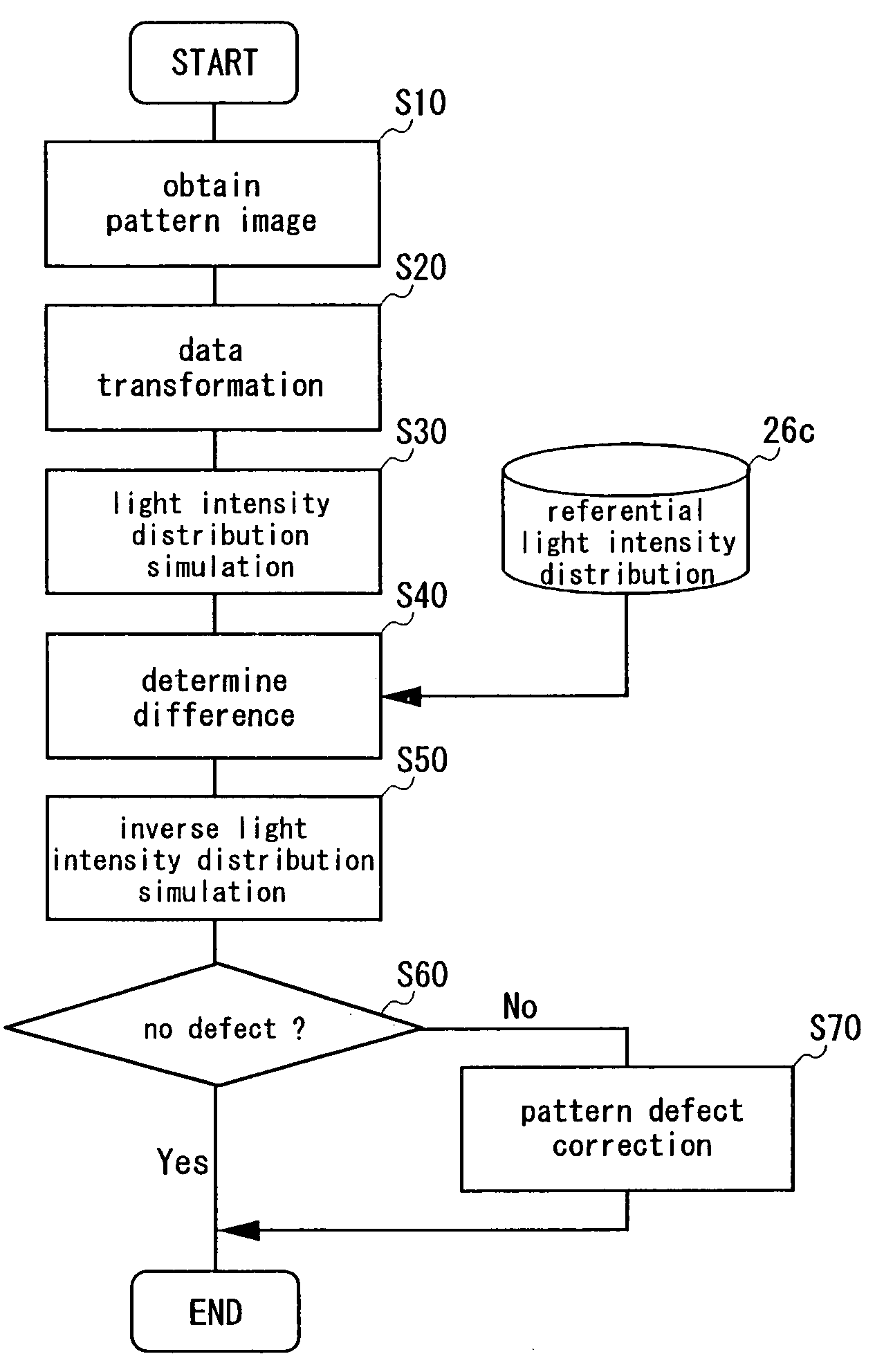
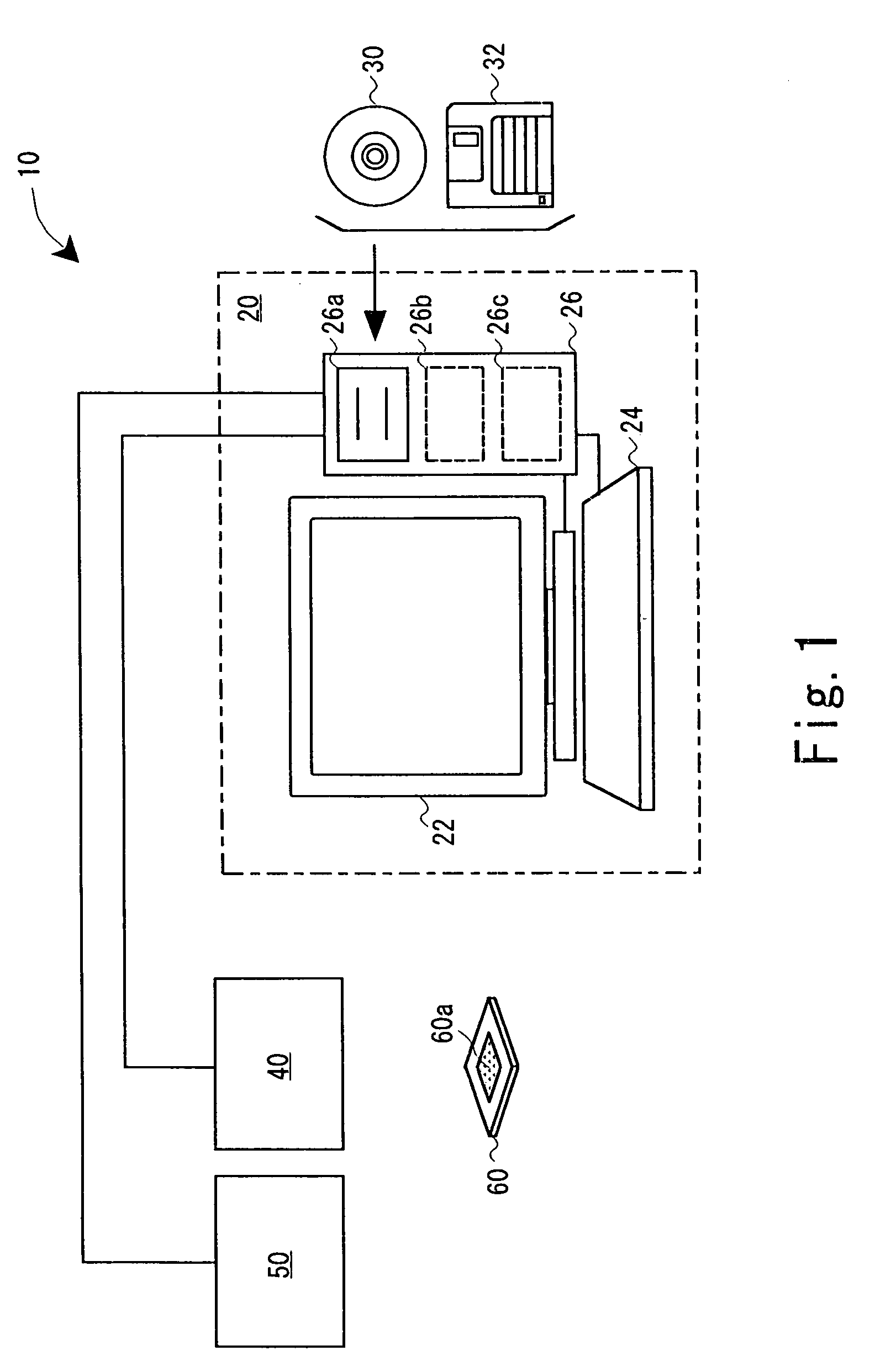
[0050]FIG. 1 shows the present invention.
[0051] A pattern inspection system 10 is constituted of a workstation 20 (control unit), a CD-ROM 30 or a flexible disk 32 in which a pattern inspection program is recorded, a scanning electron microscope 40 (hereinafter also referred to as the SEM), and a focused ion beam machining apparatus 50 (hereinafter also referred to as the FIB machining apparatus).
[0052] The workstation 20 includes a display 22 to display a screen, a keyboard 24 to provide instructions by pressing keys, and a control device 26 in which a recording medium drive device 26a, a CPU 26b and a hard disk 26c are contained. The CD-ROM 30 and the flexible disk 32 can be inserted in the recording medium drive device 26a. After the CD-ROM 30 or the flexible disk 32 is inserted in the recording medium drive device 26a, the workstation 20 follows the instruction inputted via the keyboard 24 to download the pattern inspection program which is recorded in the CD-ROM 30 or the flex...
PUM
| Property | Measurement | Unit |
|---|---|---|
| light intensity distribution simulation | aaaaa | aaaaa |
| light intensity distribution | aaaaa | aaaaa |
| inverse light intensity distribution simulation | aaaaa | aaaaa |
Abstract
Description
Claims
Application Information