Apparatus and method of dispensing photosensitive solution in semiconductor device fabrication equipment

a technology of semiconductor devices and apparatuses, applied in the direction of packaging goods, instruments, separation processes, etc., can solve the problems of photosensitive layer, adverse effects on the quality of photosensitive layer, and errors in subsequent steps of photolithographic process

Active Publication Date: 2005-10-13
SAMSUNG ELECTRONICS CO LTD
View PDF6 Cites 20 Cited by
  • Summary
  • Abstract
  • Description
  • Claims
  • Application Information

AI Technical Summary

Benefits of technology

[0018] According to the invention, the amount of air bubbles in the solution, e.g. in a photosensitive solution, is substantially reduced during the process of depositing the photosensitive solution on a wafer or the like. Thus, a uniform layer of photosensitive material can be formed on the wafer. As a result, there is less likelihood that the layer will become a cause of defects in a pattern formed on the wafer when the layer is patterned and used as an etch mask.

Problems solved by technology

However, micro bubbles may flow into line 44 through the pump 42 because the pressure of the nitrogen gas may not be sufficient to discharge the micro bubbles through the line 24 and drain valve 28.
As a result, the quality of the photosensitive layer is adversely affected.
Such a defect in the photosensitive layer may give rise to errors in subsequent steps of the photolithographic process.

Method used


Image

  • Apparatus and method of dispensing photosensitive solution in semiconductor device fabrication equipment
  • Apparatus and method of dispensing photosensitive solution in semiconductor device fabrication equipment
  • Apparatus and method of dispensing photosensitive solution in semiconductor device fabrication equipment

Examples


Embodiment Construction

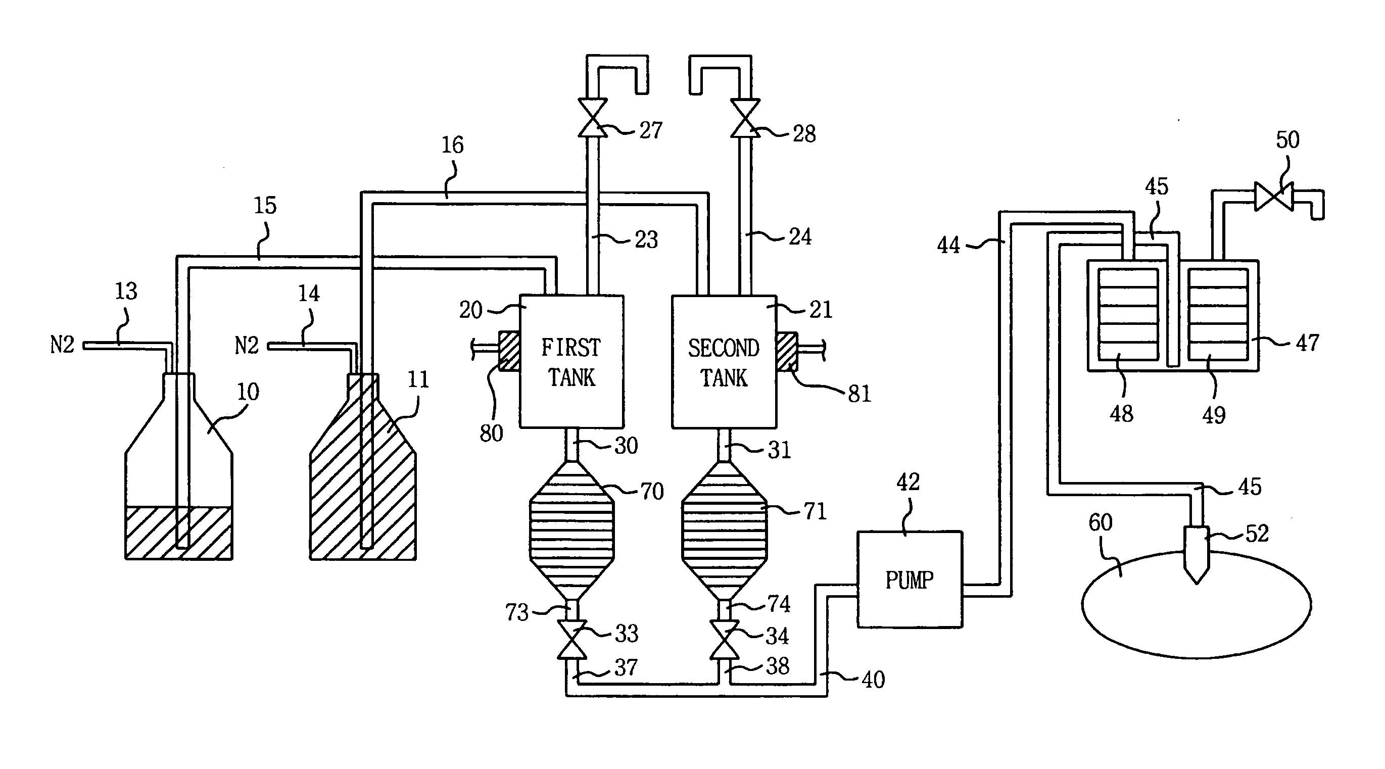
[0024] The present invention will be described in detail with reference to FIGS. 3 and 4. Like reference numerals are used to designate like elements throughout the drawings.

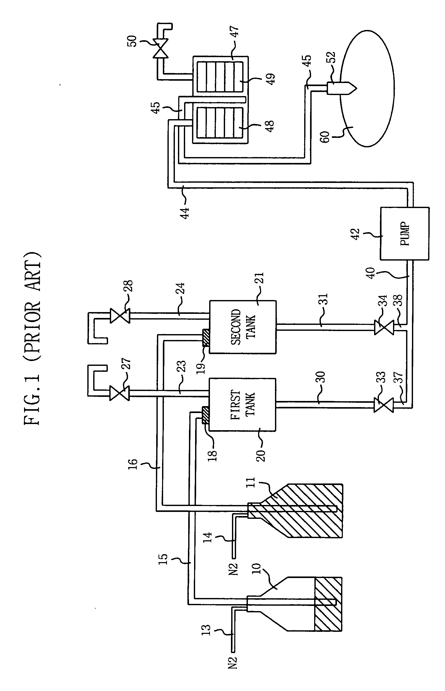
[0025] Referring first to FIG. 3, the photosensitive solution dispensing apparatus has a configuration similar to that of the prior art shown in FIG. 1 and so, only a portion of the photosensitive solution dispensing apparatus will be described again. Briefly, the photosensitive solution dispensing apparatus includes supply vessels 10 and 11, first and second tanks 20 and 21, a pump 42, a filter unit 47 including filters 48 and 49, and a nozzle 52. Similarly, lines 15 and 16 extend between and connect the supply vessels 10 and 11 and the first and second buffer tanks 20 and 21, respectively. Lines 23 and 24 and drain valves 27 and 28 are provided for discharging air and photosensitive solution from the first and second tanks 20 and 21.

[0026] In addition, though, the photosensitive solution dispensing apparatus...


PUM

PropertyMeasurementUnit
volumeaaaaaaaaaa
photosensitiveaaaaaaaaaa
thicknessaaaaaaaaaa

Abstract

A method of and apparatus for dispensing photosensitive solution. substantially reduces the amount of air bubbles in the photosensitive solution during the dispensing operation. The photosensitive solution dispensing apparatus includes at least one supply vessel that contains the solution, a respective buffer tank that buffers the solution supplied from each supply vessel, a filter unit for filtering the solution, a pump for pumping the solution pumped from the buffer tank to the filter unit, a dispensing nozzle connected to the filter unit, and a dedicated bubble removal filter that is interposed between the buffer tank and the pump. The bubble removal filter is configured to remove air bubbles from the solution before the solution flows into the pump and is dispensed through the nozzle.

Description

BACKGROUND OF THE INVENTION [0001] 1. Field of the Invention [0002] The present invention relates to semiconductor manufacturing equipment. More particularly, the present invention relates to an apparatus and method of dispensing photosensitive solution, such as photoresist, onto a semiconductor wafer. [0003] 2. Description of the Related Art [0004] The recent rapid development of information processors, such as computers, has brought about remarkable advances in semiconductor devices, e.g., in semiconductor memory devices. These devices must be highly integrated if they are to be competitive in the marketplace, i.e., if they are to be of high quality yet low in cost to manufacture. One way to achieve a high degree of integration in a semiconductor device is to scale down components of the device. For example, the thickness of a gate oxide or the channel length of a transistor of the device can be reduced. To meet the current demand for high-performance devices, semiconductor manufa...

Claims


Application Information

Patent Timeline
Patent Type & Authority Applications(United States)
IPC IPC(8): H01L21/027H01L21/00G03F7/16B65B1/04
CPCG03F7/162H01L21/6715
Inventor JANG, SUNG-KUN
Owner SAMSUNG ELECTRONICS CO LTD
Why Eureka
Try Eureka