Method and apparatus for repairing shape, and method for manufacturing semiconductor device using those

a technology of semiconductor devices and shapes, which is applied in the direction of semiconductor/solid-state device testing/measurement, semiconductor/solid-state device details, instruments, etc., can solve the problems of reducing the yield of the semiconductor manufacturing process, affecting the yield sometimes becoming fatal defects during processing of the substrate such as wafers. , to achieve the effect of reducing the cost and reducing the manufacturing time of the semiconductor device, reducing the cost of the process, and improving the yield of the front-

Inactive Publication Date: 2005-10-13
EBARA CORP
View PDF13 Cites 11 Cited by
  • Summary
  • Abstract
  • Description
  • Claims
  • Application Information

AI Technical Summary

Benefits of technology

[0037] According to the invention, the pattern shape of the substrate having the imperfect pattern can be repaired without lengthening the manufacturing time of the semiconductor device.
[0038] According to the shape repairing method and the shape repairing apparatus, the substrate pattern can be repaired in front-end of a manufacturing process of the semiconductor device, for which there has not been any practicable measure, thereby yield in the front-end of the semiconductor process can be remarkably improved. Moreover, an excellent advantage of drastic decrease in cost is obtained by applying those to the method for manufacturing the device.

Problems solved by technology

In a manufacturing process of a semiconductor device, defects occurring during processing a substrate such as wafer sometimes become fatal defects (killer defects).
As density of the device becomes higher, the defects become the killer defects in more cases even if they are microscopic defects.
Such defects cause reduction in yield in the semiconductor manufacturing process.
In particular, when the defects occur in front-end of the manufacturing process, influence on the yield is more significant.
That is, repairing the defect occurring in each step, for example, repairing open or short circuit of wiring or removing a residue in a via-hole has not been performed.
However, the density of the device becomes higher, for example, a wafer having a high density pattern having the minimum line width of 0.1 μm or less has appeared, therefore the redundant circuit is impossible to be formed.
However, repairing a shape of an imperfect pattern, for example, etching of the residue has not been performed.

Method used


Image

  • Method and apparatus for repairing shape, and method for manufacturing semiconductor device using those
  • Method and apparatus for repairing shape, and method for manufacturing semiconductor device using those
  • Method and apparatus for repairing shape, and method for manufacturing semiconductor device using those

Examples


Embodiment Construction

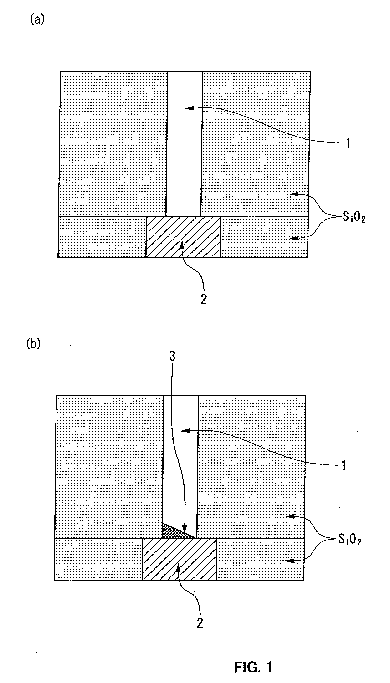
[0047] Hereinafter, an embodiment of the invention is described using a case, as an example, that the wafer is used as the substrate, the via-hole as the pattern, and the fast atom beam (FAB) as the radiation rays, and the residue in the via-hole is etched. FIG. 1 is a schematic view showing a condition that the via-hole is opened in a wiring step in a semiconductor manufacturing process. That is, FIG. 1 shows a condition that metal wiring 2 is formed, and then SiO2 is deposited using CVD (Chemical Vapor Deposition) and etched, and then a via-hole 1 is opened. FIG. 1A shows a case that the via-hole is normally opened, and FIG. 1B shows a case that the via-hole is imperfect. In FIG. 1B, a residue 3 (etching residue) is remained at a bottom of the via-hole, and when metal is filled in the via-hole using wet plating or CVD method later in that condition, the metal insufficiently contacts to an underneath metal-wiring 2, resulting in loss of functions as an element. That is, the defects...


PUM

PropertyMeasurementUnit
thicknessaaaaaaaaaa
diameteraaaaaaaaaa
diameteraaaaaaaaaa

Abstract

The invention relates to a method for enabling repair of a defect in a substrate, particularly the invention provides a method and apparatus for enabling repair of a pattern shape in a semiconductor device, which has not been able to be practiced because of lack of a suitable method, and further provides a method for manufacturing the semiconductor device using those. A method for repairing the pattern shape of a substrate having an imperfect pattern is used, which includes (a) a step for inspecting the substrate and thus detecting the imperfect pattern, and (b) a step for repairing the pattern shape by performing etching or deposition to the detected imperfect-pattern using radiation rays. Moreover, apparatus for repairing a pattern shape of a via-hole in a wafer having an imperfect via-hole is used, which has a defect inspection section for detecting the imperfect via-hole, and an etching section for etching the imperfect via-hole using a fast atom beam.

Description

BACKGROUND OF THE INVENTION [0001] 1. Field of the Invention [0002] The present invention relates to a method and apparatus for repairing a pattern of a substrate, and a method for manufacturing a semiconductor device using those. [0003] 2. Description of the Related Art [0004] In a manufacturing process of a semiconductor device, defects occurring during processing a substrate such as wafer sometimes become fatal defects (killer defects). As density of the device becomes higher, the defects become the killer defects in more cases even if they are microscopic defects. Such defects cause reduction in yield in the semiconductor manufacturing process. In particular, when the defects occur in front-end of the manufacturing process, influence on the yield is more significant. At present, the defects are not repaired in an individual step, and a method is used, wherein a redundant circuit is previously formed, and a defective circuit is broken (open) using laser so that it is not used. Th...

Claims


Application Information

Patent Timeline
Patent Type & Authority Applications(United States)
IPC IPC(8): H01L21/66C23C16/00C23F1/00G01R31/307H01L21/311H01L21/3205H01L23/52
CPCG01R31/307H01L21/31116H01L22/22H01L2924/0002H01L2924/00
Inventor SATAKE, TOHRUNOJI, NOBUHARUHATAKEYAMA, MASAHIROWATANABE, KENJI
Owner EBARA CORP
Why Eureka
Try Eureka