Imager

Inactive Publication Date: 2005-10-13
COMMISSARIAT A LENERGIE ATOMIQUE ET AUX ENERGIES ALTERNATIVES +1
View PDF4 Cites 31 Cited by
  • Summary
  • Abstract
  • Description
  • Claims
  • Application Information

AI Technical Summary

Benefits of technology

[0033] enhanced time response, i.e., the rise and fall times of the value of the signal delivered according to the variations of the illumination, more closely following the variations even when these variatio

Problems solved by technology

low image retention, and therefore allowing successi

Method used


Image

  • Imager
  • Imager
  • Imager

Examples


Embodiment Construction

[0095] As explained above, as compared with the prior art, the invention consists of replacing an amorphous material forming the active layer with polymorphous silicon.

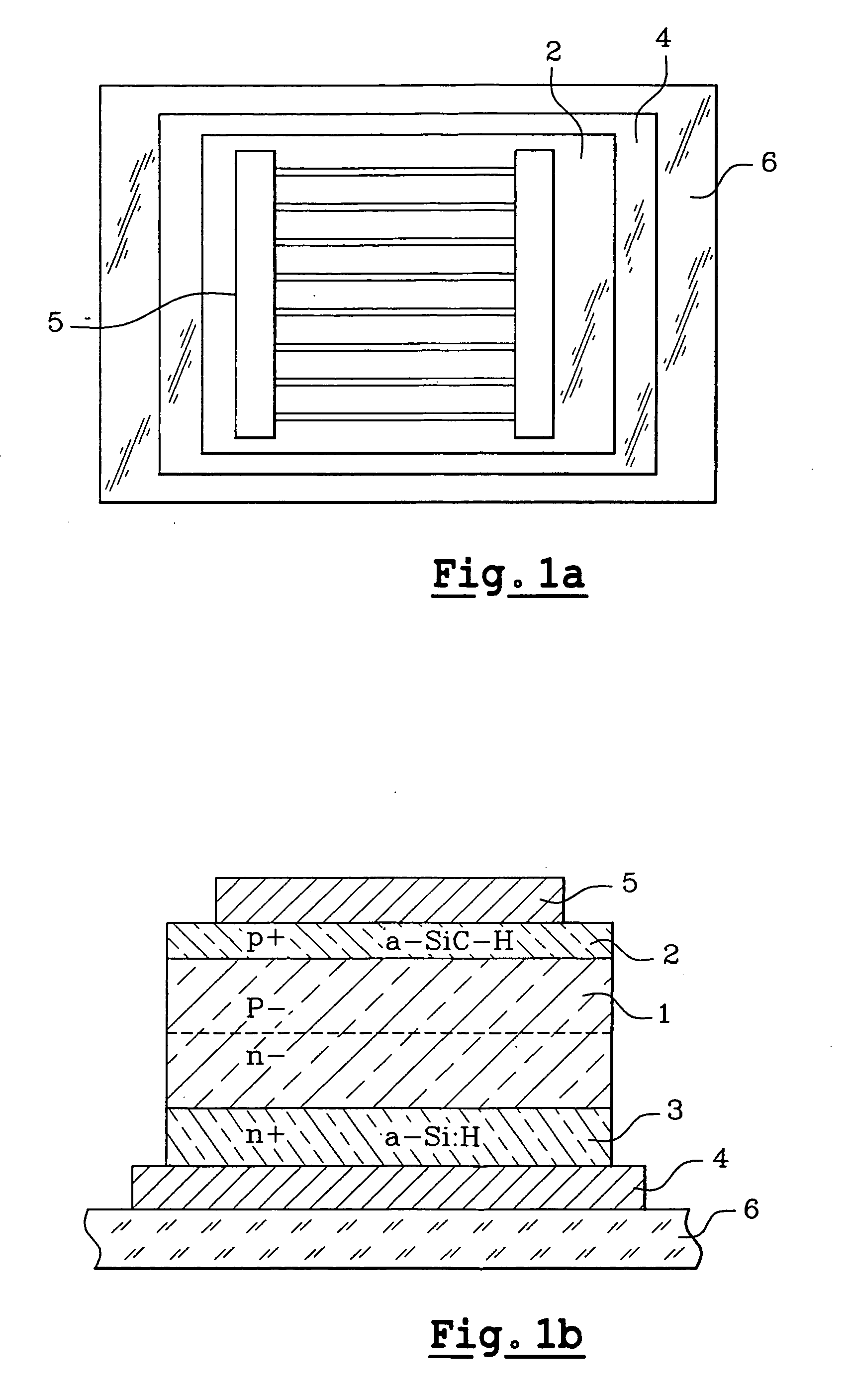
[0096] First of all, it will be pointed out how it is possible to recognize polymorphous silicon from amorphous silicon upon examining them. The structure of polymorphous silicon is schematized in FIG. 3. Polymorphous silicon includes a matrix 100 wherein aggregates and nanocrystals 101, 102, etc. n, n being larger than 102, illustrated by black spots with variable shape and size, are incorporated. With microscopy measurements, it may be shown that the matrix containing the nanocrystals has medium range order between the second and sixth neighboring atoms. The nanostructure of polymorphous silicon is also notably characterized by infrared absorption, by microscopy, Raman spectroscopy. It may also be characterized by a hydrogen exodiffusion spectrum clearly distinct from that of amorphous silicon.

[0097] For example, ...


PUM


Abstract

Assembly of sensors formed as an imager with a detection brick including a photosensitive material, a brick for addressing and optionally processing signals from the sensor(s), an interconnection brick located between the detection brick and the addressing brick, this brick including connection pads, characterized in that the photosensitive material of the detection brick contains polymorphous silicon. The invention also relates to a method for the making of the latter.

Description

TECHNICAL FIELD [0001] The invention is in the field of photosensitive sensors, in particular in the visible wavelength range, i.e. approximately between 400 and 800 nm and in the ultraviolet wavelength range, i.e. approximately between 10 and 400 nm. These sensors include a layer possibly consisting of several sublayers of a photosensitive material converting photons into electric charges. These sensors may exist in an isolated form or in the form of an assembly of sensors forming together an imager. The invention notably relates to sensors or a PIN or a NIP diode imager. STATE OF THE PRIOR ART [0002] A photosensitive sensor delivers an electrical signal, the amplitude of which, in an operating range, is an increasing monotonous function of the intensity of the light which it receives. Sensors are generally arranged in the form of a matrix of sensors formed with one or several columns, and with one or several lines. [0003] UV sensors are generally arranged in the form of isolated s...

Claims


Application Information

Patent Timeline
IPC IPC(8): H01L27/146H01L31/103
CPCH01L27/14643H01L27/14665H01L31/103
Inventor GUEDJ, CYRILALVAREZ, JOSEBONNASSIEUX, YVANKLEIDER, JEAN-PAULMOUSSY, NORBERTROCA I CABARROCAS, PERETCHAKAROV, SVETOSLAV
Owner COMMISSARIAT A LENERGIE ATOMIQUE ET AUX ENERGIES ALTERNATIVES
Why Eureka
Try Eureka