

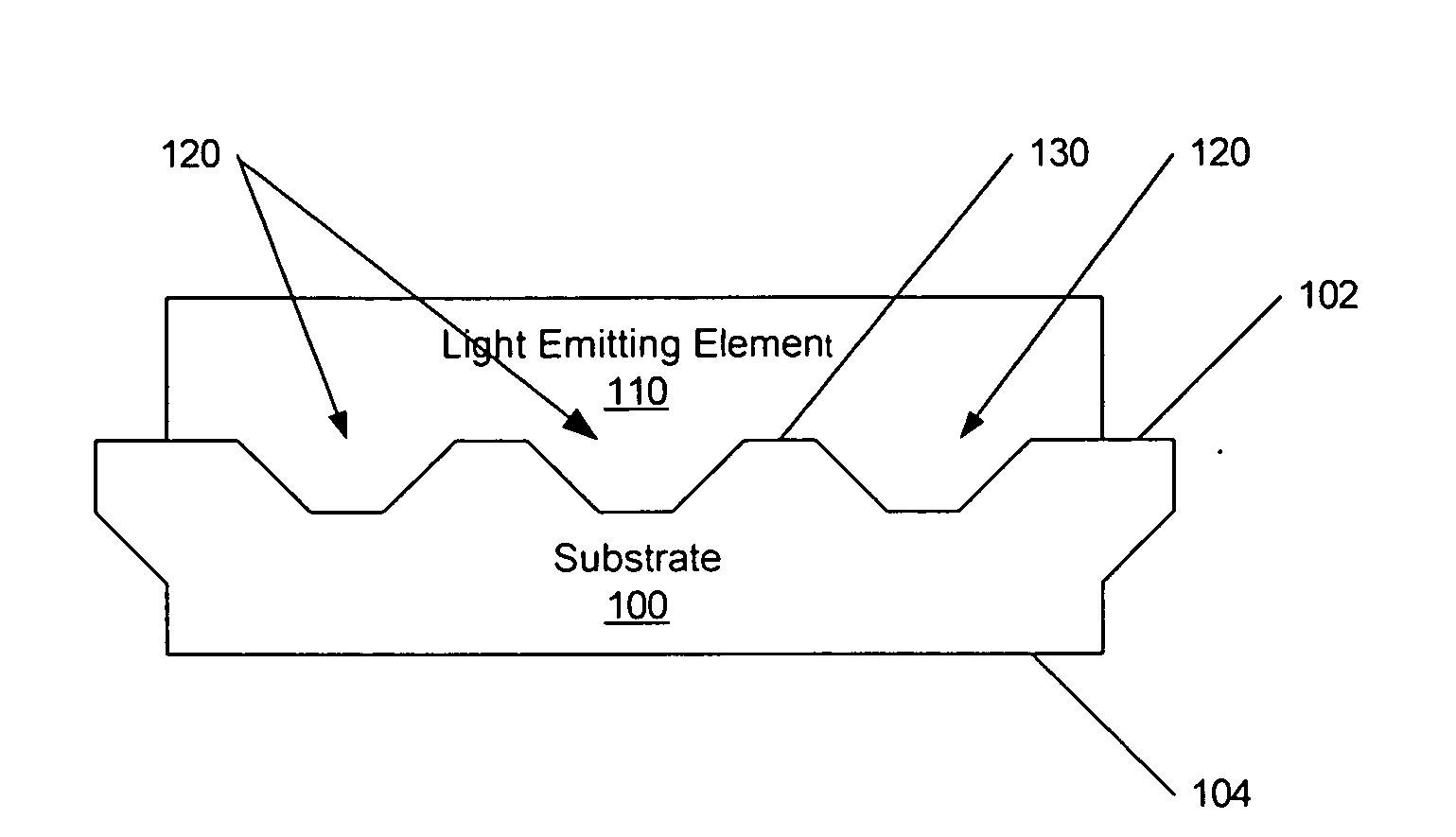
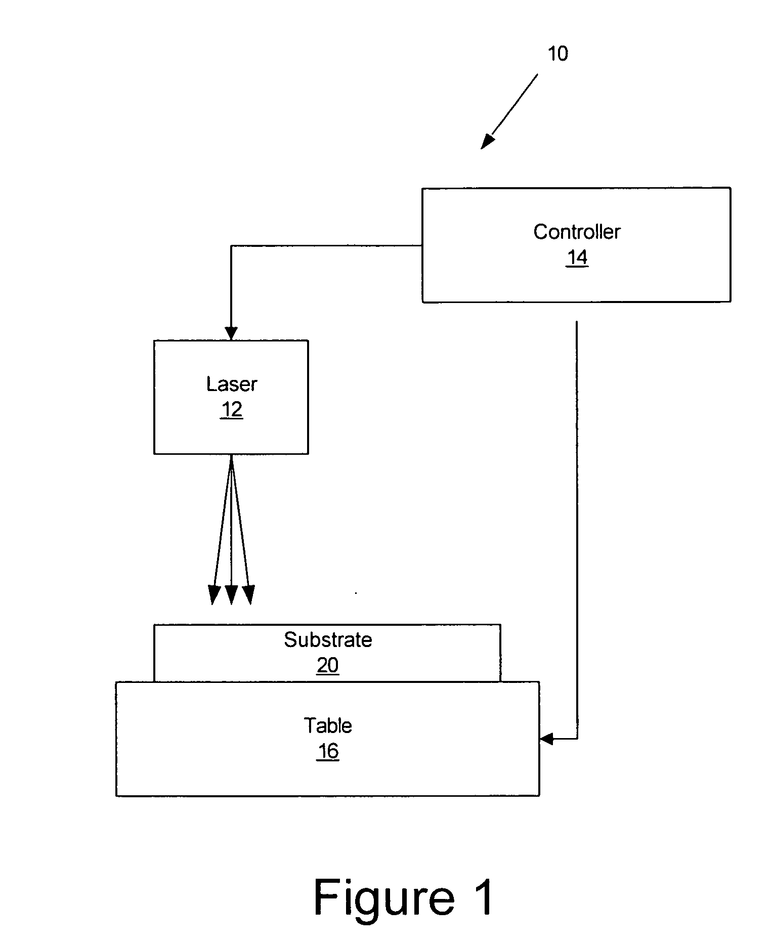
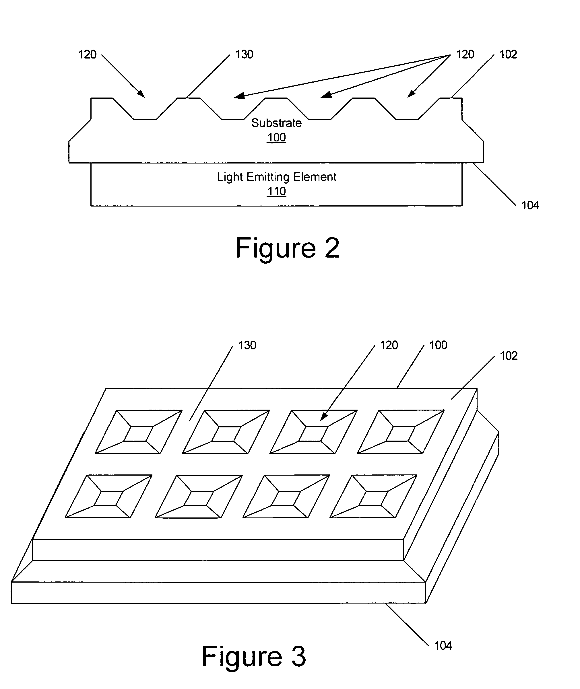
Laser patterning of light emitting devices and patterned light emitting devices
a technology of light emitting devices and laser patterns, which is applied in the direction of photomechanical treatment originals, instruments, manufacturing tools, etc., can solve the problems of reducing affecting the efficiency of conventional leds, and inability to emit all ligh
- Summary
- Abstract
- Description
- Claims
- Application Information
AI Technical Summary
Benefits of technology
Problems solved by technology
Method used
Image

Examples
examples
[0073] An excimer laser operating at 308 nm and using mask projection optics that project a 2 mm×2 mm field was used on a wafer. Using a step and repeat sequence, geometric patterns were laser scribed into the backside of a SiC LED wafer approximately 1 μm deep using 5 pulses at approximately 4.2 J / pulse. Ground control regions were left between the laser scribed regions of the wafer. Subsequent to the laser process, the wafers were aggressively etched in a RIE tool to remove any light absorbing material generated by the laser process. Because the RIE process is anisotropic, the morphology change induced by the laser was maintained. Initial test patterns were 10 μm squares, 15 μm circles, 20 μm crosses and 20 μm stars. Die from the square patterned areas showed the largest increase in light output versus die from the control region. Approximately a 20% increase was provided by a double pass interleaved square pattern over the die from the control regions.
[0074]FIGS. 14A and 15A are...
PUM
| Property | Measurement | Unit |
|---|---|---|
| Nanoscale particle size | aaaaa | aaaaa |
| Energy | aaaaa | aaaaa |
| Perimeter | aaaaa | aaaaa |
Abstract
Description
Claims
Application Information