

Method of manufacturing a semiconductor light emitting device, semiconductor light emitting device, method of manufacturing a semiconductor device, semiconductor device, method of manufacturing a device, and device
a technology of light emitting devices and semiconductors, which is applied in the direction of semiconductor lasers, crystal growth processes, polycrystalline material growth, etc., can solve the problems of deteriorating device properties, difficult to obtain substrates with reduced defects, and high defect densities, so as to achieve the effect of improving property
- Summary
- Abstract
- Description
- Claims
- Application Information
AI Technical Summary
Benefits of technology
Problems solved by technology
Method used
Image

Examples
first embodiment
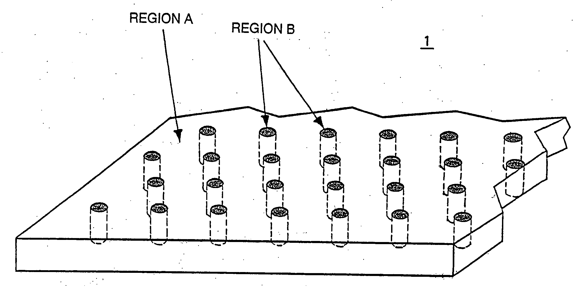
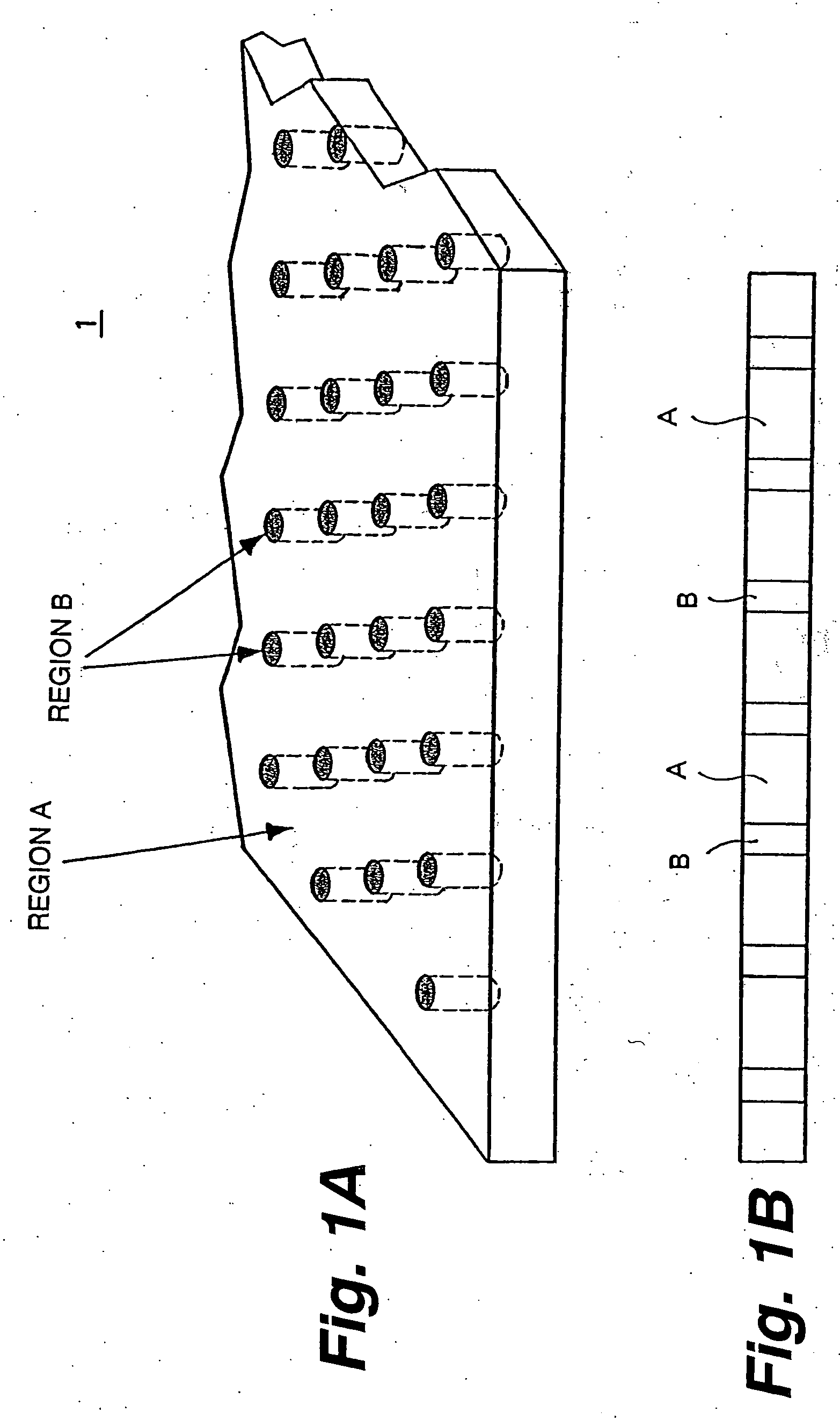
[0172]FIG. 6 is a plan view showing the GaN substrate used in the Perspective and cross-sectional views of the GaN substrate 1 appear as shown in FIGS. 1A and 1B. The GaN substrate 1 is an n-type substrate having a (0001) plane (C-plane) orientation. The GaN substrate 1, however, may be of an R-plane, A-plane or M-plane orientation. In the GaN substrate 1, regions B composed of a crystal having a high average dislocation density periodically align in form of hexagonal lattices in the region A having a low average dislocation density. In this case, the straight line connecting nearest two regions B coincides with the orientation of GaN or its equivalent. Alternatively, the straight line connecting nearest two regions B may coincide with the orientation or its equivalent of GaN. The regions B penetrate the GaN substrate 1. Thickness of the GaN substrate 1 is 200˜600 μm, for example. Broken lines in FIG. 6 are shown only for demonstrating relative positional relations among the regi...
second embodiment
[0207] Next explained is the invention.
[0208] As shown in FIG. 12, in the second embodiment, both the shorter sides and the longer sides of the rectangular device region 2, which form border lines of each device region 2, are straight lines connecting centers of regions B unlike the first embodiment. Here again, the laser stripes 3 lie on lines connecting midpoints of shorter sides of individual device regions 2. In this manner, transfer of influence of the regions B to the emission regions can be prevented.
[0209] The second embodiment is different from the first embodiment in forming cavity mirrors by dicing the substrate by cleavage along the-border lines of the device regions 2 that are straight lines connecting centers of regions B.
[0210] The regions B having more dislocations are considered easier to break than the region A. Therefore, when the substrate is diced along the straight lines that connect regions B, the regions B function as perforation, and the region A is clearl...
third embodiment
[0214] Next explained is the invention.
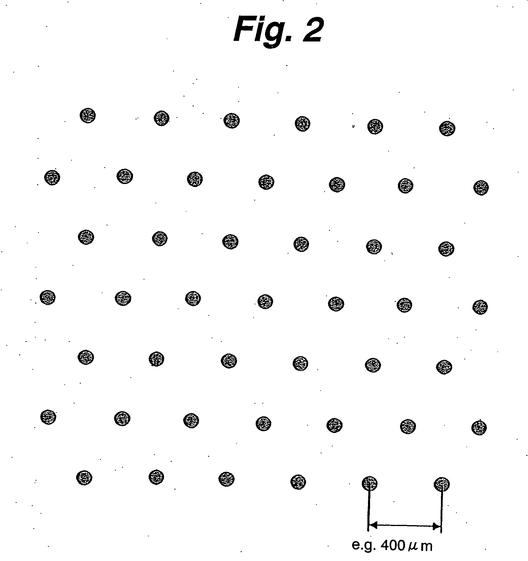
[0215] In the third embodiment, as shown in FIG. 14, regions B made of a crystal having a higher average dislocation density are aligned periodically in form of rectangular lattices in the region A having a lower average dislocation density in a GaN substrate 1. A single rectangle having regions B at its four corners is defined as a single device region 2. In this case, each straight line connecting nearest two adjacent regions B in the lengthwise direction of the rectangle coincides with the orientation of GaN, and each straight line connecting nearest two adjacent regions B and being one of shorter side of the rectangle coincides with the orientation of GaN.
[0216] Interval of regions B in the lengthwise direction of the rectangular lattices is 600 μm, for example, and interval of regions B in the direction parallel to the shorter sides of the rectangular lattices is 400 μm, for example. In this case, each device region 2 is sized 600×400 μ...
PUM
| Property | Measurement | Unit |
|---|---|---|
| Diameter | aaaaa | aaaaa |
| Diameter | aaaaa | aaaaa |
| diameter | aaaaa | aaaaa |
Abstract
Description
Claims
Application Information