Multilayer printed board, electronic apparatus, and packaging method

a multi-layer printed board and electronic equipment technology, applied in the direction of printed element electric connection formation, waveguide type devices, waveguides, etc., can solve the problems of insufficient capacitance of capacitors of currently available buried capacitance boards, increased dielectric constants of materials, and increased cost of materials whose dielectric constant is improved, so as to improve the character of the capacitive coupling layer

Inactive Publication Date: 2005-10-20
FUJITSU LTD
View PDF7 Cites 12 Cited by
  • Summary
  • Abstract
  • Description
  • Claims
  • Application Information

AI Technical Summary

Benefits of technology

[0038] As described above, according to the present invention, the characteristics of the capacitive coupling layer can be improved to shift the resonance point to a high frequency domain.

Problems solved by technology

However, a capacitance of the capacitor of the currently-available buried capacitance board is insufficient.
Therefore, there is a problem in that an impedance of about several tens of MHz becomes higher to reduce a bypass effect.
However, a material whose dielectric constant is improved is generally expensive.
A high dielectric constant material is not easily available in many cases.
However, when the dielectric is too thin, a withstand voltage between the power supply layer and the ground layer reduces and they are short-circuited at worst.
In addition, when the dielectric is too thin, handling thereof is hard.
However, because of a limitation of size of a device, the area of the capacitor portion in the printed board is limited in many cases.

Method used


Image

  • Multilayer printed board, electronic apparatus, and packaging method
  • Multilayer printed board, electronic apparatus, and packaging method
  • Multilayer printed board, electronic apparatus, and packaging method

Examples


first embodiment

Mode

[0090] Hereinafter, a multilayer printed board according to a first embodiment mode of the present invention will be described with reference to FIG. 1 to FIG. 13.

Structure

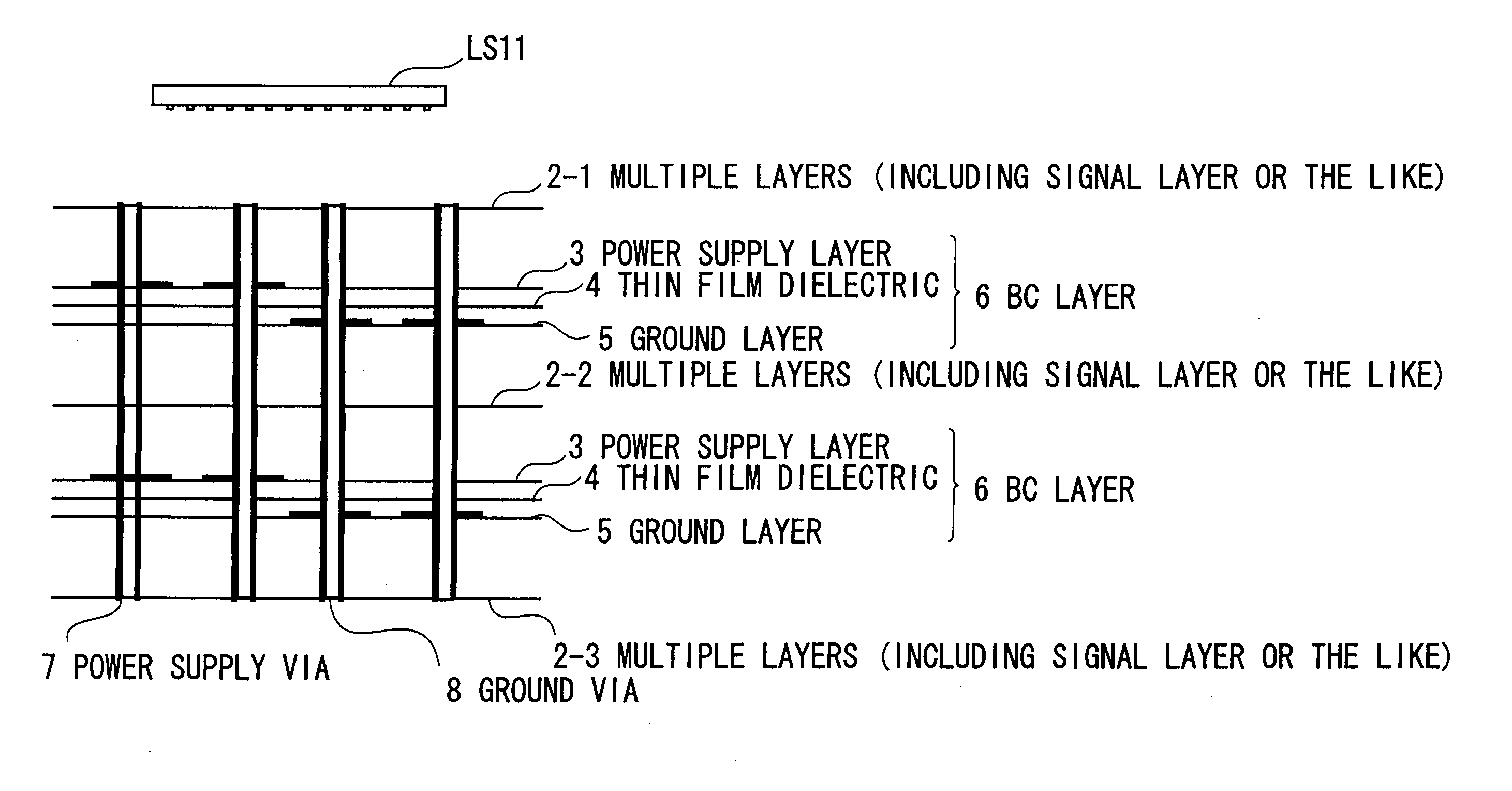
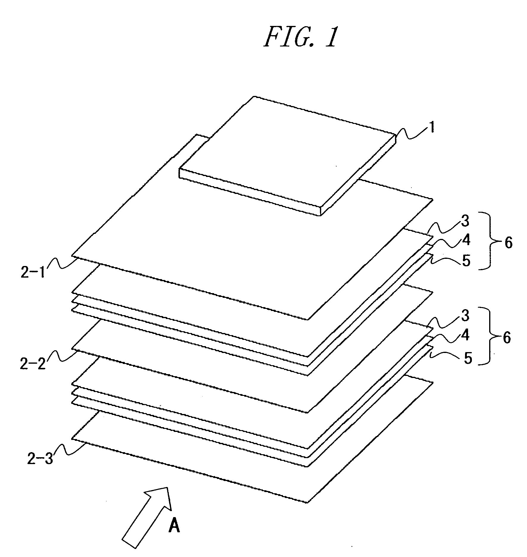
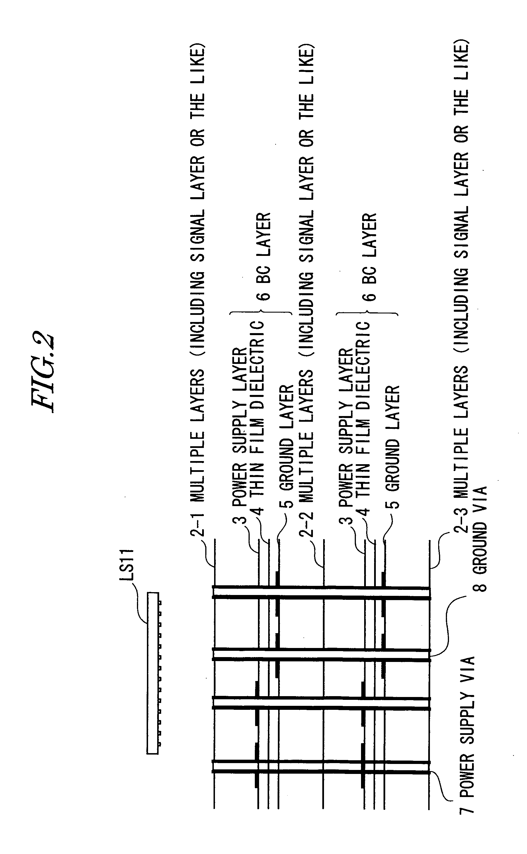
[0091]FIG. 1 is a perspective view showing an example of the multilayer printed board. FIG. 2 is a front view in the case where the multilayer printed board is viewed from a direction indicated by an arrow A in FIG. 1. As shown in FIG. 1 or FIG. 2, the multilayer printed board includes an element such as an LSI 1, printed boards 2-1, 2-2, and 2-3, each of which has a signal layer connected with the element, and BC layers 6 located between the printed boards 2-1 and 2-2 and the printed boards 2-2 and 2-3.

[0092] The printed boards 2-1, 2-2, 2-3, etc. each are composed of a single or plural printed boards. In the case of plural items, they are referred to as multiple layers 2-1, 2-2, 2-3, etc. In general, each of the printed boards 2-1, 2-2, 2-3, etc. includes a conductive layer (this is referred to as the sig...

embodiment 1

[0106]FIG. 3 and FIG. 4 show a structure of a multilayer printed board according to Embodiment 1 of the present invention. In this embodiment, numerical analytical results obtained by calculation of a modeled multilayer printed board are shown. FIG. 3 is a front view showing an analytical model in the case where the multilayer printed board is viewed from the front (for example, the direction indicated by the arrow A in FIG. 1) as in FIG. 2.

[0107] As shown in FIG. 3, the multilayer printed board includes an insulator 2A, a power supply layer 3-1, a thin film dielectric 4-1, a ground layer 5-1, an insulator 2B, a power supply layer 3-2, a thin film dielectric 4-2, a ground layer 5-2, and an insulator 2C. Note that a signal layer is formed on an upper side of the insulator 2A or a lower side of the insulator 2B in an original multilayer printed board. In this embodiment, the influence of the signal layer is not considered for the simplification of the model.

[0108] Each of the insula...

embodiment 2

[0148]FIG. 8 and FIG. 9 show Embodiment 2. In Embodiment 1, the number of power supply vias 7B is made equal to the number of ground vias 8. They are increased from one set (V1G1-1) to five sets (V1G1-5) by one and the impedance characteristic of the BC layers 6 are calculated. In Embodiment 2, a ratio between the number of power supply vias 7B and the number of ground vias 8 is set to 1:2. Such a combination is increased from one set to four sets and the impedance characteristic of the BC layers 6 are calculated. Other structures are identical to those in Embodiment 1.

[0149]FIG. 8 shows the position of the power supply pin of the LSI 1 (power supply via 7A) and the positions of the power supply vias 7B and the ground vias 8 in this embodiment. As shown in FIG. 8, even in any of V1G2-1 to V1G2-4, a pair of ground vias 8 are provided on both sides of each of the power supply vias 7 to make one set.

[0150] In the case of V1G2-1, the one set is provided on the left side of the power s...


PUM


Abstract

A multilayer printed board comprising a plurality of capacitive coupling layers (6) each consisting of a dielectric layer (4) and a power supply layer (3) and a ground layer (5) facing each other while sandwiching the dielectric layer (4), first vias (7) connecting between the power supply layers (3) included in the plurality of capacitive coupling layers (6), and second vias (8) connecting between the ground layers (5) included in the plurality of capacitive coupling layers (6).

Description

[0001] This is a continuation of Application PCT / JP2003 / 001010, filed on Jan. 31, 2003.BACKGROUND OF THE INVENTION [0002] 1. TECHNICAL FIELD [0003] The present invention relates to a printed wiring board and an electronic apparatus including the printed wiring board. [0004] 2. BACKGROUND ART [0005] In a printed board on which a high-speed element is mounted, there are problems in that a high frequency current flows into a power supply layer and a ground layer, with the result that resonance occurs and an unnecessary electromagnetic wave is emitted. Up to now, a configuration to which a circuit using a resistor and a magnetic material is added has been employed to suppress the resonance. [0006] However, such a method is disadvantageous in taking measures for packaging in a narrow space. The use of the resistor and the magnetic material increases the number of parts. [0007] Up to now, for resonance measures or noise measures, high-frequency connection is made between the power supply ...

Claims


Application Information

Patent Timeline
Patent Type & Authority Applications(United States)
IPC IPC(8): H01L23/498H01P3/08H05K1/11H05K1/16H05K3/42H05K3/46
CPCH01L23/49822H01L2224/16H01L2924/09701H01L2924/3011H01P3/088H05K1/0298H05K1/112H05K1/115H05K1/162H05K3/429H05K3/4641H05K2201/0175H05K2201/0179H05K2201/093H05K2201/09309H05K2201/10674H01L23/50
Inventor KOYAMA, HIDEKI
Owner FUJITSU LTD
Why Eureka
Try Eureka