LSI package provided with interface module, and transmission line header employed in the package

a technology of interface module and package, applied in the field of lsi package, can solve the problems of inherently high inside operation speed of signal processing lsi, lower processing lsi, further operation speed, etc., and achieve the effect of high frequency characteristics

Inactive Publication Date: 2005-10-20
KK TOSHIBA
View PDF1 Cites 80 Cited by
  • Summary
  • Abstract
  • Description
  • Claims
  • Application Information

AI Technical Summary

Benefits of technology

[0010] In view of these situations, it is an object of the present invention to provide an LSI package which can be manufactured through the existing production line and is not accompanied by an extremely complicated configuration, with high frequency characteristics and to provide an LSI package which implements part of the above-mentioned LSI package and a transmission line header which implements part of the above-mentioned LSI package.

Problems solved by technology

However, the operation speed on a printed circuit board level mounting the signal processing LSI is still lower than the operation speed inside the signal processing LSI, although the inside operation speed of the signal processing LSI is inherently high, and further, on a rack level packaging hierarchy implemented by the printed circuit boards, the operation speed becomes further lower.
The above-mentioned operation speed problems are caused by increases in transmission loss, noise, and electromagnetic interference associated with the electrical interconnections, which increase as the operation frequency becomes higher.
Therefore, such a tendency that the packaging technology limits the operation speed of the system rather than the operation speed of the signal processing LSI, has become more and more significant recently in the electrically interconnected device.
In the above-mentioned earlier technology, it is difficult to carry out board mounting of an interposer in an actual interposer mounting process, since the board mounting of an interposer is carried out under the condition where an interposer is mingled with an I / F module.
For instance, since the I / F module has an optical transmission line such as an optical fiber, etc, it is not possible to give heat treatment by putting the optical fiber into a solder reflow furnace of the interposer as it is.
The problem is not limited to a case in which the optical transmission line is employed, since the same problem arises when an electrical transmission line such as a small coaxial cable is used for the transmission line.
However, in the detachable optical connector methodology, protectors for protecting optical semiconductor elements and optical connectors from mechanical damage and pollution are required.
Because of these requirements, there was a problem being that the mounting condition of other parts which are supposed to be mounted on the same board do not meet with the mounting condition of the I / F module and that existing board assembly equipment was not able to be applied to as they were.
Furthermore, the configuration becomes more and more complicated because pressure mechanism and holding mechanism of the optical connector must be provided in the detachable optical connector methodology, and therefore, the manufacturing cost drastically increases.

Method used


Image

  • LSI package provided with interface module, and transmission line header employed in the package
  • LSI package provided with interface module, and transmission line header employed in the package
  • LSI package provided with interface module, and transmission line header employed in the package

Examples


first embodiment

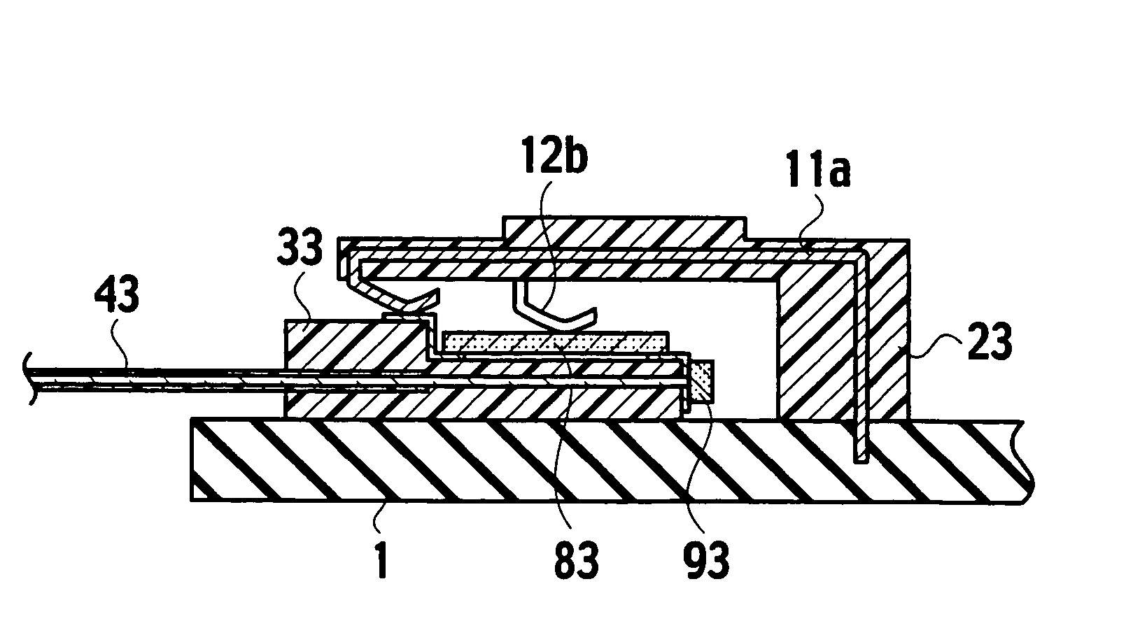
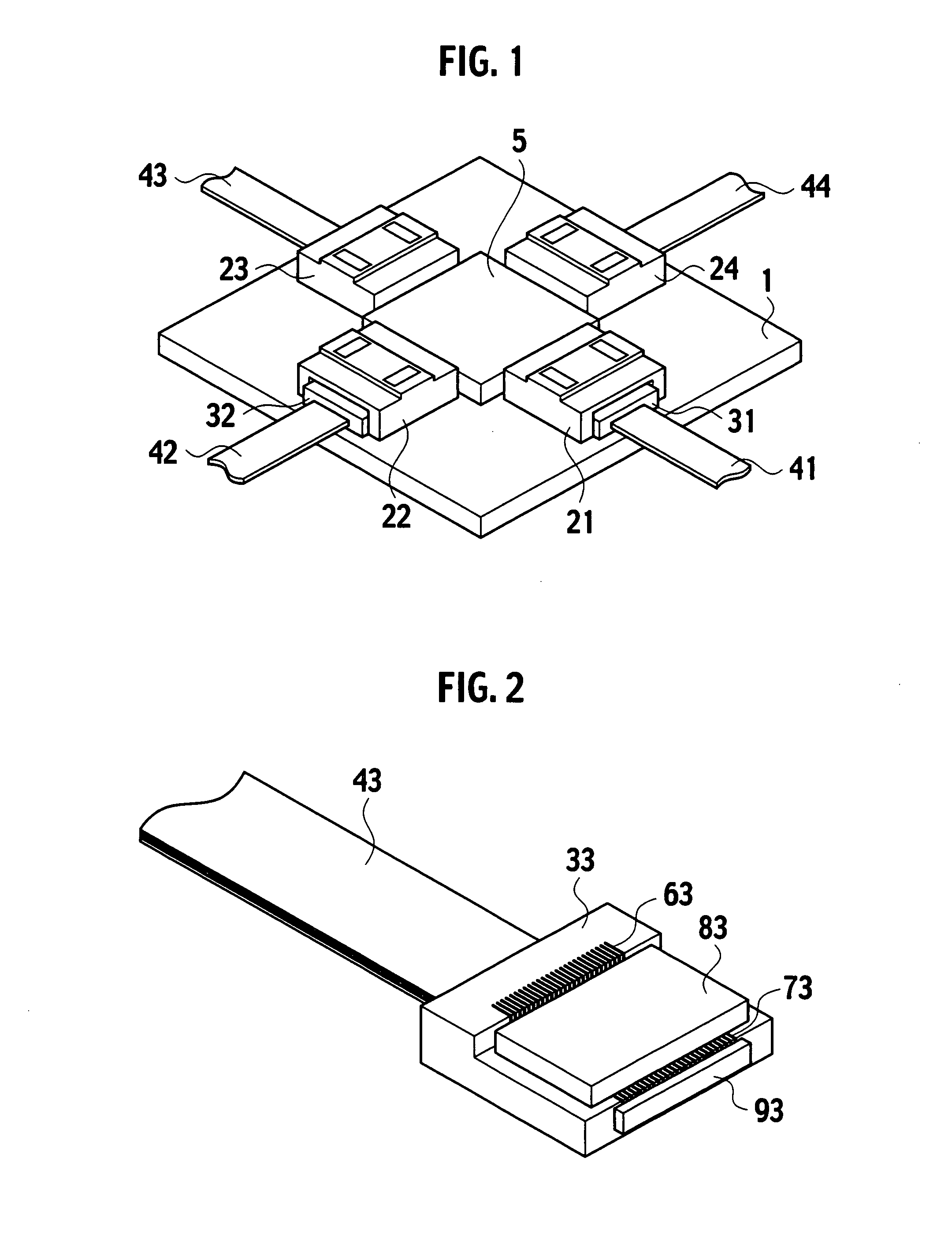
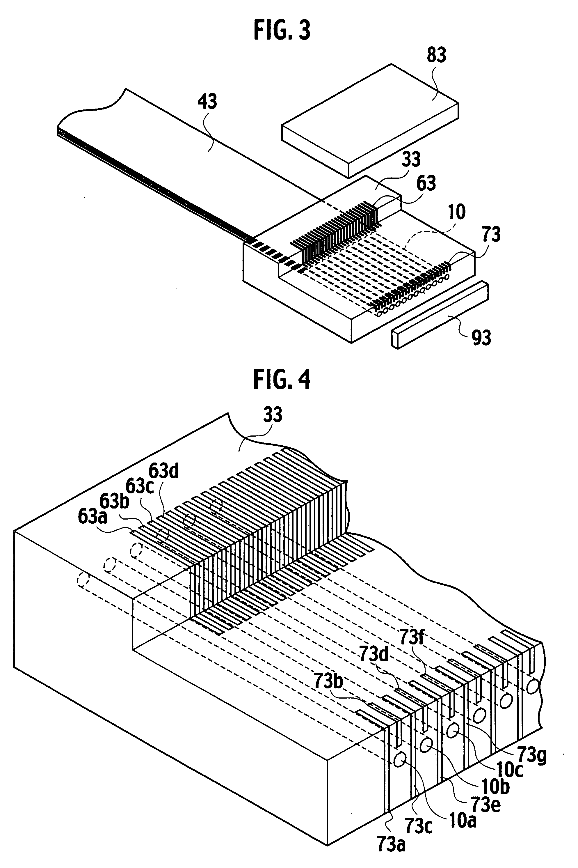
[0049] As shown in FIG. 1, the LSI package according to the first embodiment of the present invention includes a signal processing LSI chip (hereinafter called “an LSI chip”) 5, and an interposer substrate 1, on which the LSI chip 5 is mounted, configured to be electrically connected to a printed wiring board, and a plurality of receptacles (socket receptacles) 21, 22, 23, 24, which are mounted on the interposer substrate 1. Each of the receptacles 21, 22, 23, 24 implements part of an interface mechanism between signals from / to the LSI chip 5 and signals from / to external transmission lines.

[0050] The LSI package according to the first embodiment of the present invention further includes a plurality of transmission line headers implemented by the header-bodies 31, 32, . . . , each of which is configured to be inserted in corresponding receptacles 21, 22, 23, 24, respectively. On each of the header-bodies 31, 32, . . . an interface IC chip 83 is mounted so as to implement the transmi...

second embodiment

[0109] As shown in FIG. 17, a configuration of an LSI package according to a second embodiment of the present invention provided with the I / F modules simplified so as to adaptable to a case in which heat radiation of the interface IC chip 83 is comparatively small, namely the generated heat is so small that enough heat can be transported away to the interposer substrate 1 and the printed wiring board (not shown). As shown in FIG. 17, a header-base 33 according to the second embodiment is similar to the header-bodies 31, 32, . . . according to the first embodiment, with regard that the geometry, which is based on a concave heptahedron (L-type block) cutting part of a chip-mounting face prepared for mounting the interface IC chip 83, from a rectangular parallel-piped. However, in the header-base 33 according to the second embodiment, a plurality of thermal vias 417 are established alternately in each interval of an arrangement of the optical fibers 10a, 10b, 10c, . . . along vertical ...

third embodiment

[0117] As shown in FIG. 18, an LSI package according to a third embodiment of the present invention, includes a header-base 33 encompassing a topology which turns the header-base 33 of the second embodiment upside down. Namely, as shown in FIG. 18, the header-base 33 according to the third embodiment is an insulating supporting body based on a concave heptahedron (L-type block) which is formed by cutting part of the chip-mounting face prepared for mounting the interface IC chip 83, in a lower-left part of a rectangular parallel-piped. As easily understood from FIG. 18, the chip-mounting face is connected to a receptacle-contacting face disposed at the most upper level through a level difference (sidewall face) extending vertically to the receptacle-contacting face. Electrical terminals 416 extend from the chip-mounting face to the receptacle-contacting face through the level difference. The electrical terminals 416 are external-extraction electrodes for electrically connecting the h...


PUM


Abstract

An LSI package encompasses a transmission line header embracing a header-base, a transmission line held by the header-base, and an interface IC chip mounted on the header-base, an interposer substrate having a plurality of board-connecting joints, which facilitate connection with the printed wiring board; an LSI chip mounted on the interposer substrate; and a receptacle having a lead terminal and being mounted on the interposer substrate, configured to accommodate the transmission line header so that the interface IC chip electrically connects to the LSI chip through the lead terminal.

Description

CROSS REFERENCE TO RELATED APPLICATIONS AND INCORPORATION BY REFERENCE [0001] This application is based upon and claims the benefit of priority from prior Japanese Patent Application P200 4-100734 filed on Mar. 30, 2004; the entire contents of which are incorporated by reference herein. BACKGROUND OF THE INVENTION [0002] 1. Field of the Invention [0003] The present invention relates to an LSI package provided with an interface (I / F) module, an interposer and an I / F module which are used in the LSI package, and a transmission line header implementing the I / F module. [0004] 2. Description of the Related Art [0005] With improvements in the performance of electrically interconnected devices such as bipolar transistors and field-effect transistors, remarkable developments in the operation speed is being attempted in large scale integrated circuits for signal processing (hereinafter described “signal processing LSI”). However, the operation speed on a printed circuit board level mounting ...

Claims


Application Information

Patent Timeline
Patent Type & Authority Applications(United States)
IPC IPC(8): G02B6/42H01L21/60H01L23/40H01L23/02H01L25/04H01L25/18
CPCG02B6/4201G02B6/4202H01L2924/1305H01L2224/29386H01L2224/29355H01L2224/29344H01L2224/29339H01L2924/01322H01L2924/3011H01L2924/09701H01L2924/01079H01L2924/01078H01L2224/92125H01L2224/83851H01L2224/83102H01L2224/16H01L24/83G02B6/4249H01L2924/3512H01L2924/00H01L2924/00014H01L2924/01022H01L2924/0665H01L2924/12042H01L2924/12043H01L2924/14H01L2224/05573H01L2224/05568H01L2224/05624H01L2224/05647G02B6/4251G02B6/428G02B6/4269G02B6/4284H01L24/05F16D65/0043F16D65/092F16D55/226
Inventor FURUYAMA, HIDETOHAMASAKI, HIROSHI
Owner KK TOSHIBA
Why Eureka
Try Eureka