Multi-stage curing of low K nano-porous films

a nanoporous film, multi-stage technology, applied in the direction of machines/engines, semiconductor/solid-state device details, transportation and packaging, etc., can solve the problems of reducing the response time of the device, increasing the parasitic capacitance between the device and the device structure, and destroying the device structur

Inactive Publication Date: 2005-10-20
APPLIED MATERIALS INC
View PDF30 Cites 66 Cited by
  • Summary
  • Abstract
  • Description
  • Claims
  • Application Information

AI Technical Summary

Benefits of technology

[0011] Embodiments in accordance with the present invention relate to multi-stage curing processes for chemical vapor deposited low K materials. In certain embodiments, a combination of electron beam irradiation and thermal exposure steps may be employed to control selective outgassing of porogens incorporated into the film, resulting in...

Problems solved by technology

The high temperatures at which some thermal CVD processes operate can damage device structures having layers previously formed on the substrate.
However, the barrier/liner layers typically have dielectric constants that are greater than about 2.5, and the high dielectric constants result in a combined insulator that may not significantly reduce the dielectric constant.
Additionally, the smaller device geometries result in an increase in parasitic capacitanc...

Method used


Image

  • Multi-stage curing of low K nano-porous films
  • Multi-stage curing of low K nano-porous films
  • Multi-stage curing of low K nano-porous films

Examples


examples

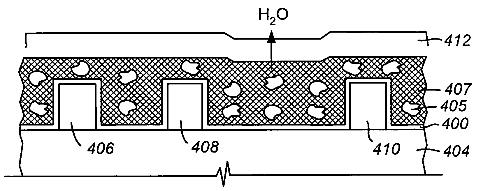
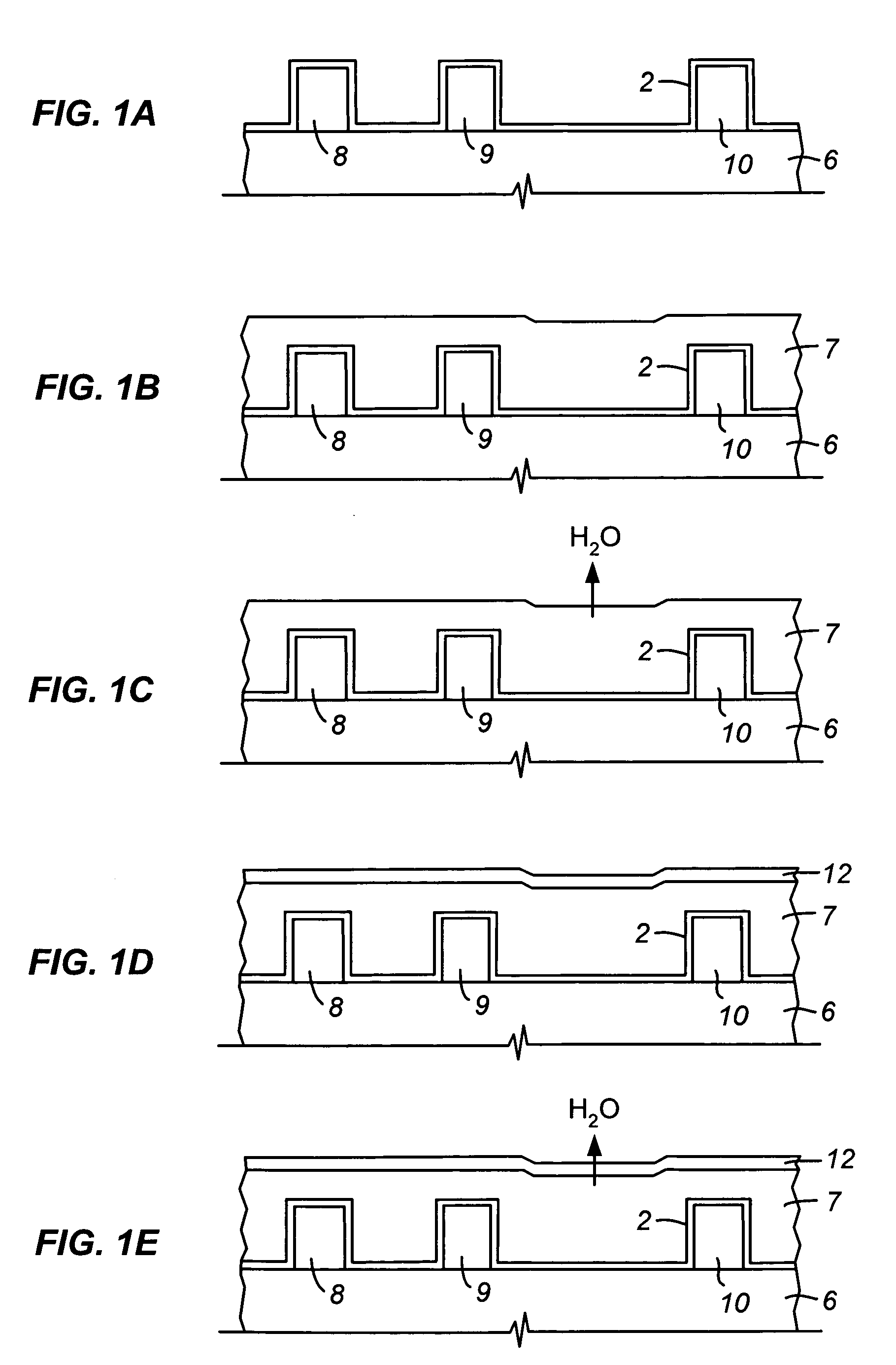
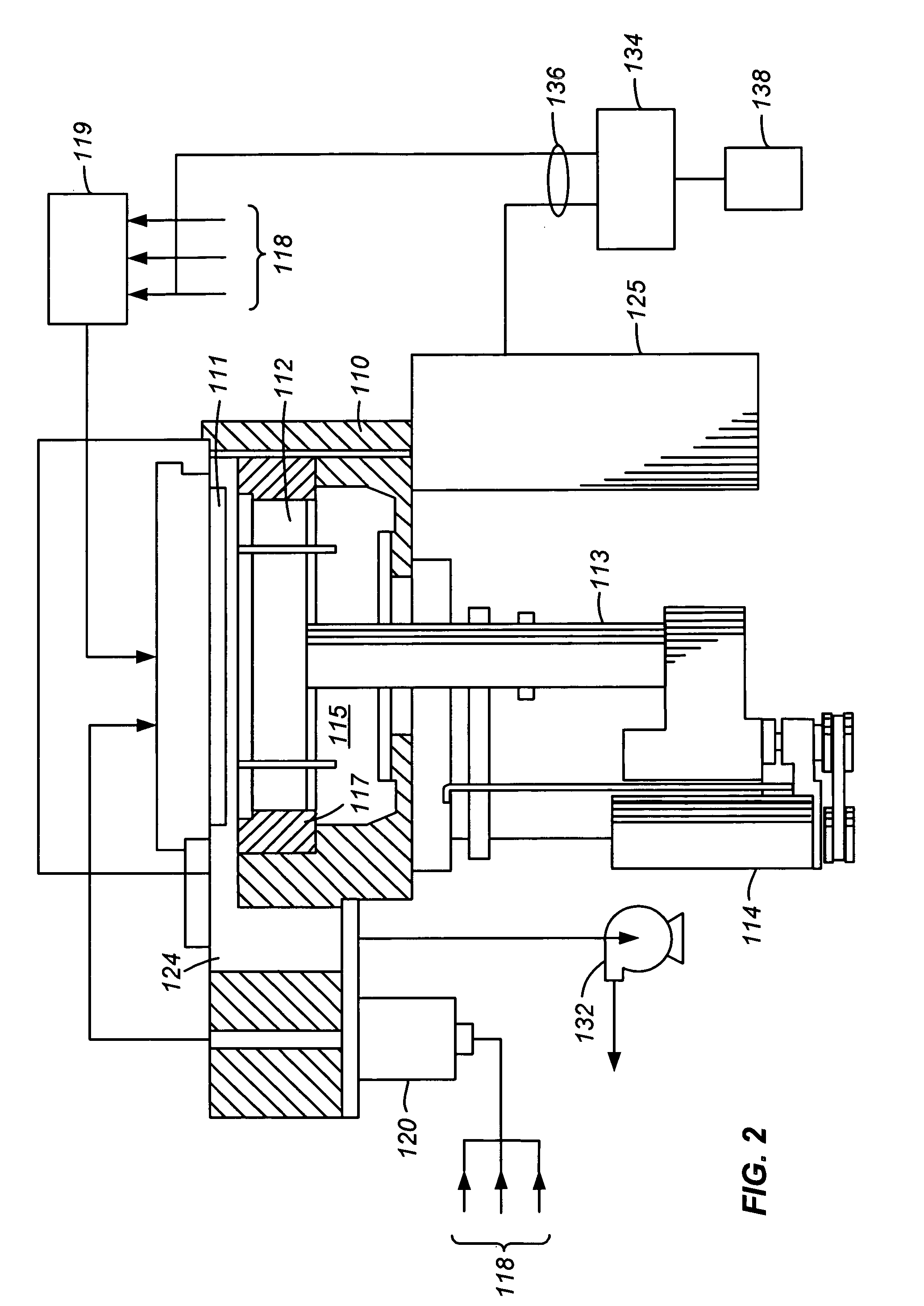
[0126] The following examples demonstrate deposition of a nano-porous silicon oxide based film having dispersed microscopic gas voids. This example is undertaken using a chemical vapor deposition chamber, and in particular, a CENTURA “DLK” system fabricated and sold by Applied Materials, Inc., Santa Clara, Calif.

Silicon Compound Having Silicon Containing and Thermally Labile Imparting Components (Hypothetical)

[0127] A nano-porous silicon oxide based film is deposited at a chamber pressure of 1.0 Torr and temperature of 30° C. from reactive gases which are vaporized and flown into the reactor as follows:

methylsilyl-2-furyl ether, at 150 sccmnitrous oxide (N2O), at1000 sccm

[0128] Prior to entering the chamber, the nitrous oxide is dissociated in a microwave applicator that provides 2000 W of microwave energy. The substrate is positioned 600 mil from the gas distribution showerhead and the reactive gases are introduced for 2 minutes. The substrate is then heated over a time period...


PUM

PropertyMeasurementUnit
Temperatureaaaaaaaaaa
Timeaaaaaaaaaa
Temperatureaaaaaaaaaa

Abstract

Embodiments in accordance with the present invention relate to multi-stage curing processes for chemical vapor deposited low K materials. In certain embodiments, a combination of electron beam irradiation and thermal exposure steps may be employed to control selective outgassing of porogens incorporated into the film, resulting in the formation of nanopores. In accordance with one specific embodiment, a low K layer resulting from reaction between a silicon-containing component and a non-silicon containing component featuring labile groups, may be cured by the initial application of thermal energy, followed by the application of radiation in the form of an electron beam.

Description

CROSS-REFERENCES TO RELATED APPLICATIONS [0001] This nonprovisional patent application claims priority to U.S. Provisional Patent Application No. 60 / 558,366, filed Mar. 31, 2004, the entire disclosure of which is incorporated herein by reference for all purposes.BACKGROUND OF THE INVENTION [0002] One of the primary steps in the fabrication of modern semiconductor devices is the formation of metal and dielectric films on a substrate by chemical reaction of gases. Such deposition processes are referred to as chemical vapor deposition or CVD. Conventional thermal CVD processes supply reactive gases to the substrate surface where heat-induced chemical reactions take place to produce a desired film. The high temperatures at which some thermal CVD processes operate can damage device structures having layers previously formed on the substrate. A preferred method of depositing metal and dielectric films at relatively low temperatures is plasma-enhanced CVD (PECVD) techniques such as describ...

Claims


Application Information

Patent Timeline
IPC IPC(8): C23C16/40C23C16/50C23C16/56H01L21/3105H01L21/312H01L21/316H01L21/469H01L21/768H01L23/52
CPCC23C16/401H01L21/76825H01L21/02126H01L21/02203H01L21/02208H01L21/02274H01L21/02304H01L21/02351H01L21/02362H01L21/3105H01L21/3121H01L21/31695H01L21/76811H01L21/76813H01L21/7682C23C16/56H01L2221/1047Y10T428/249978C23C16/505H01L21/68714F04D17/168H01L21/02365
Inventor SCHMITT, FRANCIMARZHENG, YIYIM, KANG SUBAHN, SANG H.D'CRUZ, LESTER A.HO, DUSTIN W.DEMOS, ALEXANDROS T.XIA, LI-QUNWITTY, DEREK R.M'SAAD, HICHEM
Owner APPLIED MATERIALS INC
Why Eureka
Try Eureka