

Process for improving the emission of electron field emitters
a technology of electron field and emission, which is applied in the manufacture of discharge tube main electrodes, electric discharge tube/lamps, electrode systems, etc., can solve the problems of difficult to reliably produce these displays in sizes larger than that suitable, requires relatively large electrical power to operate, and single-wall carbon nanotube films showed less emission stability than multi-wall carbon nanotube films. , the effect of good adhesion to the substra
- Summary
- Abstract
- Description
- Claims
- Application Information
AI Technical Summary
Benefits of technology
Problems solved by technology
Method used
Image

Examples
example 1
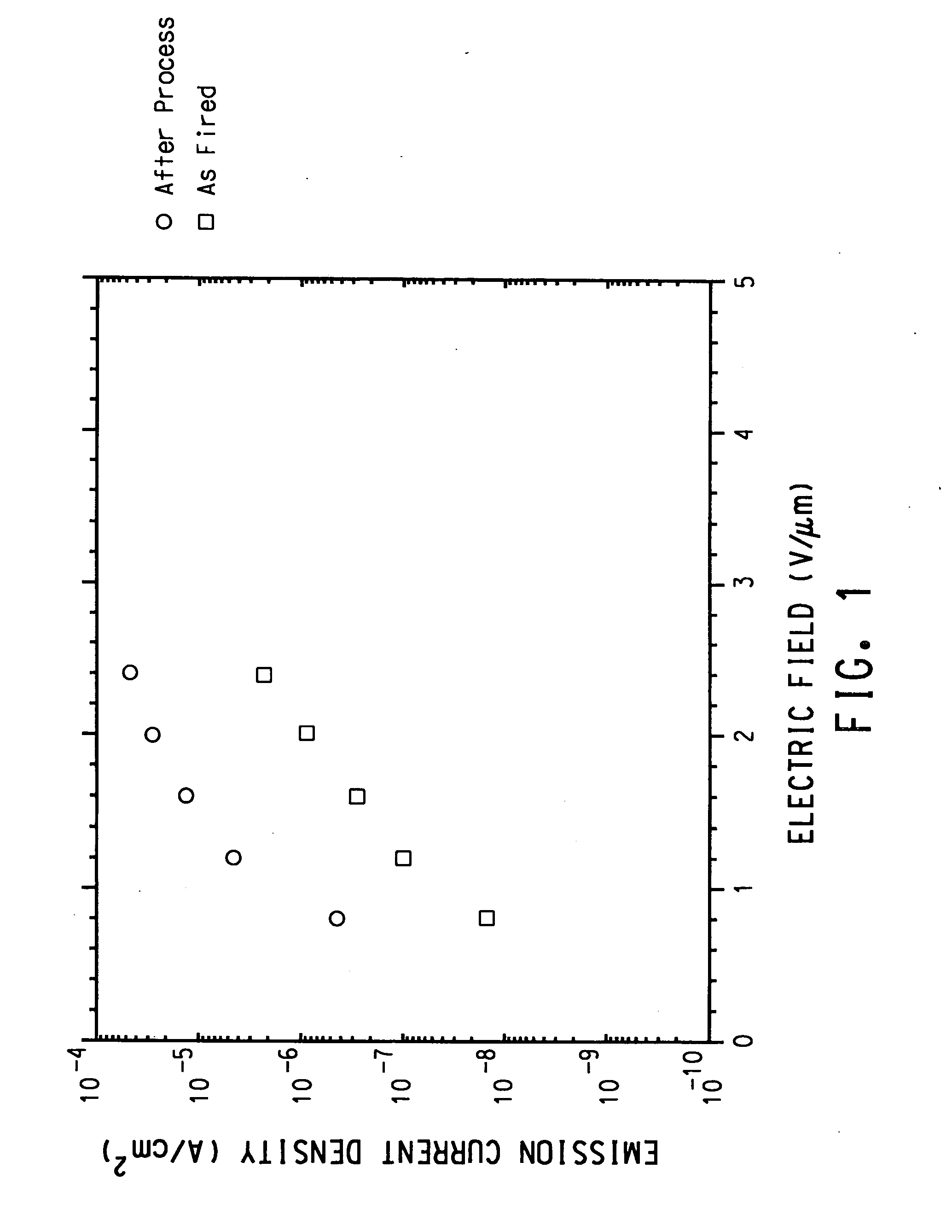
[0056] This Example demonstrates the good emission exhibited by an electron field emitter comprised of single wall carbon nanotubes after undergoing the process of the invention for improving emission.
[0057] Laserablation grown single wall nanotubes were obtained from Tubes@Rice, Rice University, Houston, Tex. as a suspension in water. 20 ml of this suspension was diluted with 40 ml of distilled water and milled on a media mill for 2 hours. The resultant material was centrifuged for 2 hours at 5000 rpm and the supernatant liquid removed. A sludge remained which was found to contain 5% nanotube solids by a thermogravimetric analysis determination. 1 gram of this material was added to 0.05 grams of a glass frit, Bayer PK 8701 (CAS Registry No. 65997-18-4) and 1.5 grams of a typical organic medium composed primarily of ethylcellulose in terpineol. These ingredients were mixed on a glass plate muller for 75 rotations to form the emitter paste. A pre-fired silvered glass substrate was p...
example 2
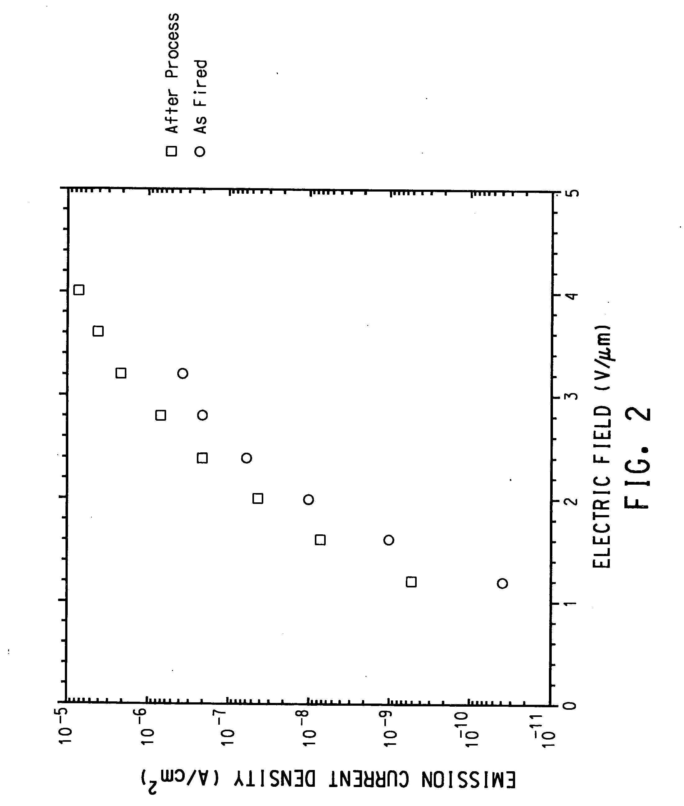
[0058] This Example demonstrates the good emission exhibited by an electron field emitter comprised of single wall carbon nanotubes after undergoing the process of the invention for improving emission.
[0059] Carbolex AP-Grade single wall carbon nanotubes were obtained as a powder from Carbolex Inc., Lexington, Ky. 0.11 gram of this material was added to 0.75 grams of a typical organic medium composed primarily of ethylcellulose in terpineol. These ingredients were mixed on a glass plate muller for 75 rotations to form the emitter paste. A pre-fired silvered glass substrate was prepared by screen printing a mixture of silver powder and a low melting glass frit in a typical organic ethylcellulose-based medium onto glass, followed by firing at 525° C. A 1 cm2 square pattern of emitter paste was then screen printed onto the pre-fired silvered glass substrate using a 325 mesh screen and the sample was subsequently dried at 120° C. for 10 minutes. The dried sample was then fired in nitro...
example 3
[0060] This Example demonstrates the good emission exhibited by an electron field emitter comprised of catalytically grown carbon fibers after undergoing the process of the invention for improving emission.
[0061] Catalytically grown carbon fibers were obtained as a powder from Catalytic Materials Ltd, 12 Old Stable Drive, Mansfield, Mass. 0.1513 grams of these catalytically grown carbon fibers were added to 0.1502 grams of glass, Bayer PK 8701 (CAS Registry No. 65997-18-4), and 1.5012 grams of a typical organic medium composed primarily of ethylcellulose in terpineol. These ingredients were mixed on a glass plate muller for 75 rotations to form the emitter paste. A pre-fired silvered glass substrate was prepared by screen printing a mixture of silver powder and a low melting glass frit in a typical organic ethylcellulose-based medium onto glass, followed by firing at 525° C. A 1 cm2 square pattern of emitter paste was then screen printed onto the pre-fired silvered glass substrate ...
PUM
 Abstract
Description
Claims
Application Information