System and method for forming multi-component dielectric films

a dielectric film and multi-component technology, applied in chemical vapor deposition coatings, electrical equipment, coatings, etc., can solve the problems of increasing power dissipation, current leakage, chemical and thermal instability of materials on silicon, etc., and achieve the effect of increasing the densities of traps

Inactive Publication Date: 2005-10-20
AVIZA TECHNOLOGY INC
View PDF29 Cites 141 Cited by
  • Summary
  • Abstract
  • Description
  • Claims
  • Application Information

AI Technical Summary

Problems solved by technology

However, as traditional silicon-based transistor geometries reach a critical point where the silicon dioxide gate dielectric becomes just a few atomic layers thick, tunneling of electrons will become more prevalent leading to current leakage and increase in power dissipation.
Unfortunately, these materials are chemically and thermally unstable on silicon, unlike silicon dioxide, forming defects and charge traps at the interface between the metal dielectric and the silicon substrate.
The charge traps and defects absorb the voltage applied at the gate and perturb the performance and reliability of the transistor.
The silicon dioxide interface buffers the silicon substrate from the dielectric, but the silicon dioxide interface may not be compatible with the surface properties of the dielectric.
Prior art deposition techniques for fabricating films such as chemical vapor deposition (CVD) are increasingly unable to meet the requirements of advanced thin films.
While CVD processes can be tailored to provide conformal films with improved step coverage, CVD processes often require high processing temperatures.
For instance, one of the obstacles of making high k gate dielectrics is the formation of an interfacial silicon oxide layer during CVD processes.
Another obstacle is the limitation of prior art CVD processes in depositing ultra thin films for high k gate dielectrics on a silicon substrate.
This approach of building up layers of different laminate films leads to many electron traps in the film due to the multiple interfaces which requires high temperature thermal anneal to fix the traps.
The addition of the high temperature thermal annealing step increases cost and time for manufacturing semiconductors, and moreover can result in the undesirable out migration of elements from previously formed layers on the wafer.
In addition, it is difficult to control the stoichiometric composition of multi-component films in the laminate method.
The dielectric constant (k), crystallization temperature and refractive index of HfSiOx films cannot be easily controlled by the traditional one chemical sequential precursor pulse methods (such as the laminate method).
Furthermore, the cycle times needed to form a film of desired thickness using the conventional sequential pulse and purge of one chemical precursor at a time are impractical and require too much time for future IC manufacturing.
Attempts to fabricate a multi-component films using mixed precursors have been limited to the traditional CVD methods.
There are however several drawbacks associated with the method described in the '613 and '734 patents.
In addition, even if appropriate volumes of samples are provided, there is no guarantee that the mixture will vaporize uniformly since each precursor has a unique boiling point, vapor pressure and volatility.
Furthermore, if the discrepancy in boiling points between the precursors is substantial, one precursor may decompose at the boiling point of the second forming particulates or contaminants.
Generally, either the precursors have not been adequately mixed, resulting in a non-uniform film composition, or mixing of the two vapors causes pre-reaction in the gas phase, resulting in the formation of particles or contaminants that are deposited on the wafer.

Method used


Image

  • System and method for forming multi-component dielectric films
  • System and method for forming multi-component dielectric films
  • System and method for forming multi-component dielectric films

Examples


Embodiment Construction

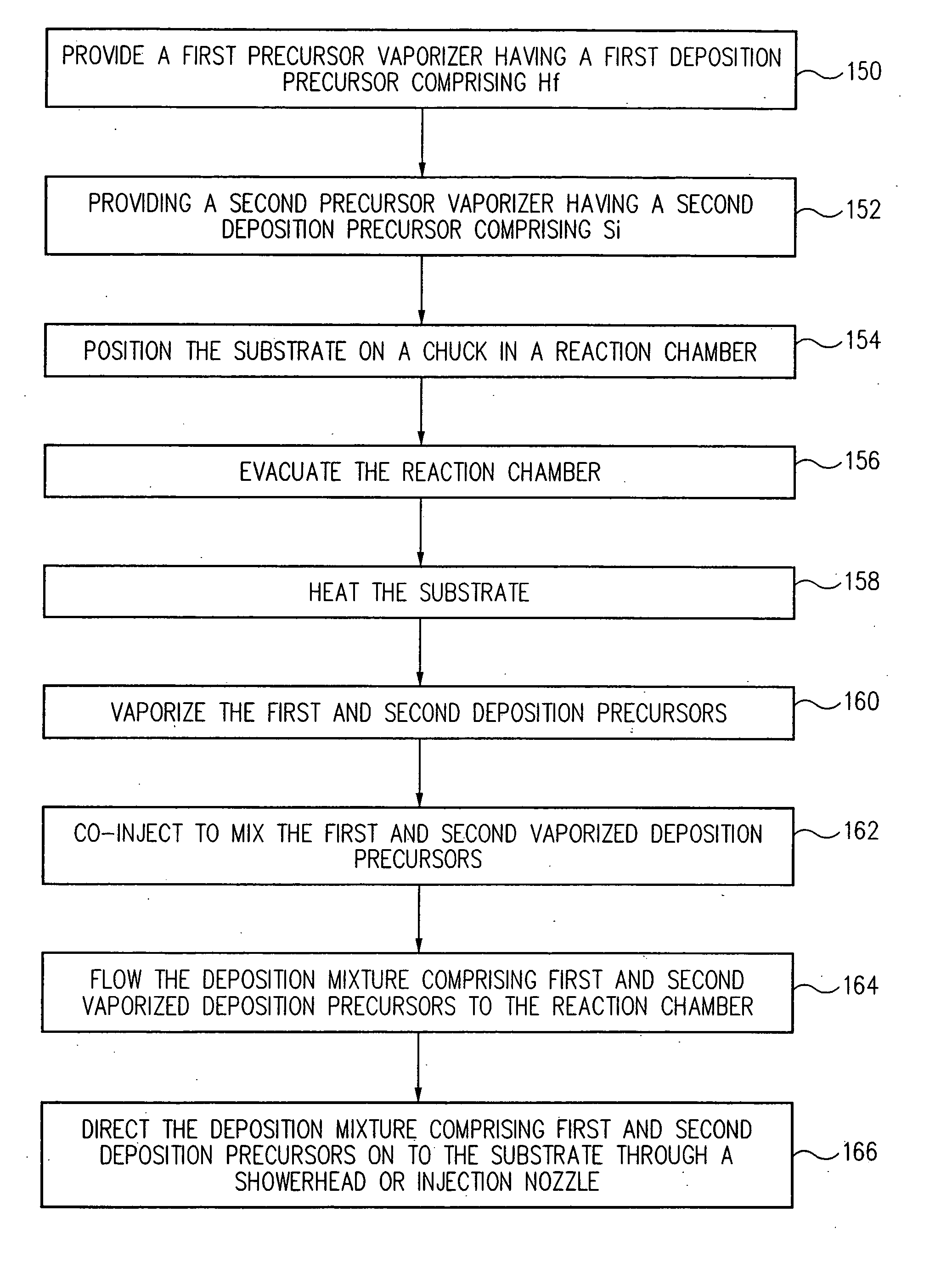
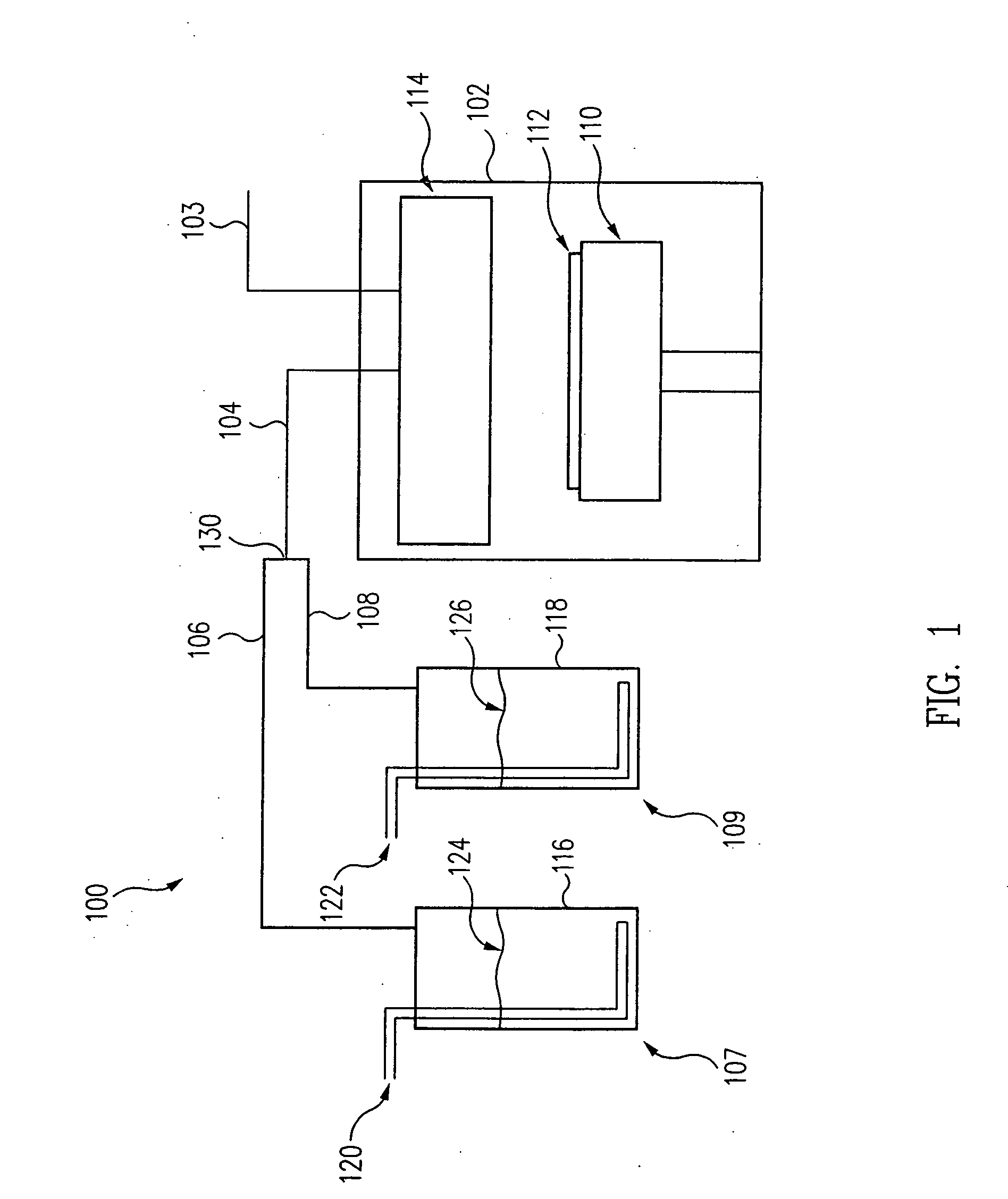
[0036] In general, the inventors have discovered a method that provides for mixing precursors such that a mixture of precursors are present in a chamber during a single pulse step in an atomic layer deposition (ALD) process to form a mono-layer having multiple chemical compounds on the surface of a substrate. The precursors are comprised of different chemical components, and such components will form the multi-component film. The inventors refer to this method as “co-injection ALD.” Such a method is a departure from the prior art, where the vaporized precursors are conveyed or pulsed separately into the chamber in the ALD process. A variety of multi-component films may be formed by the present invention, including but not limited to: metal, metal alloy, mixed metal oxides, silicates, nitrides, oxynitrides, and mixtures thereof.

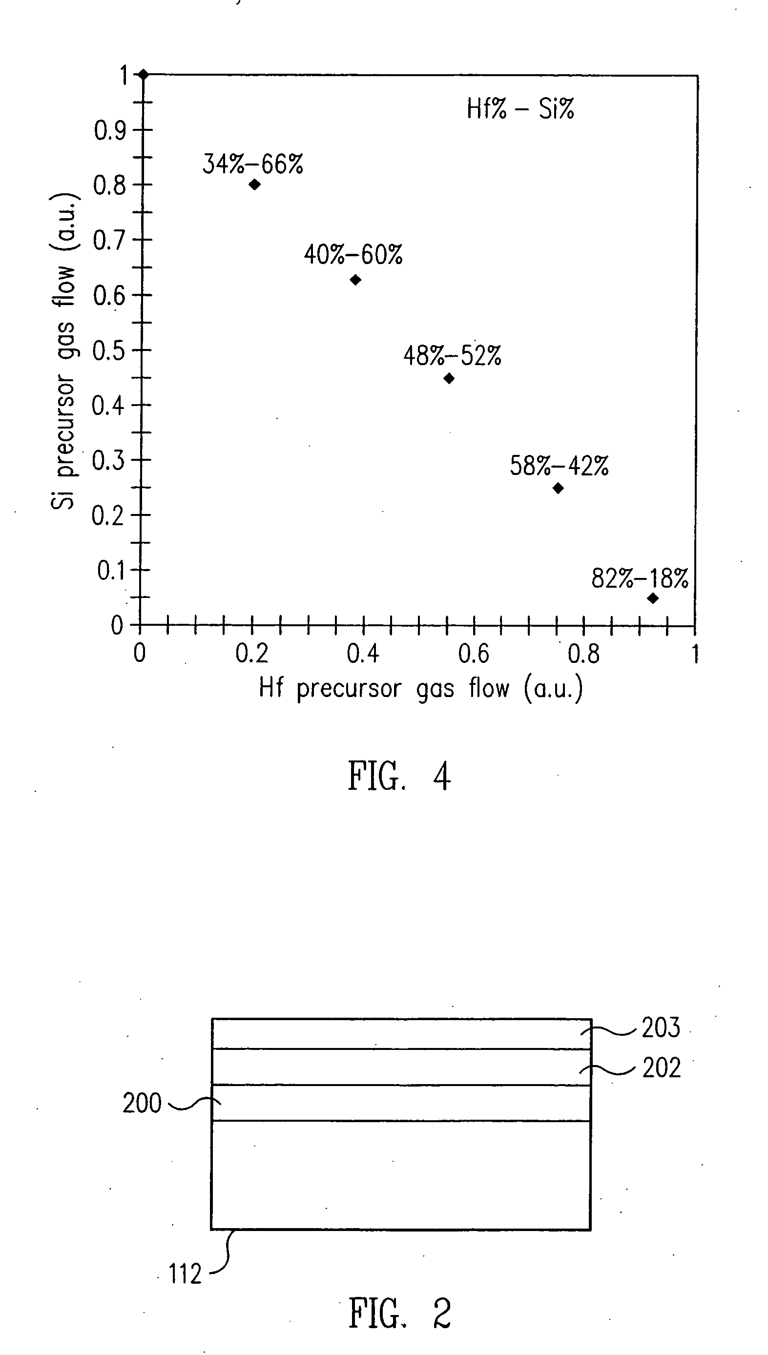
[0037] In one aspect the present invention provides a system and method for reproducibly and substantially uniformly controlling the stoichiometric compositi...


PUM

PropertyMeasurementUnit
pressureaaaaaaaaaa
dielectric thicknessaaaaaaaaaa

Abstract

The present invention provides systems and methods for mixing precursors such that a mixture of precursors are present together in a chamber during a single pulse step in an atomic layer deposition (ALD) process to form a multi-component film. The precursors are comprised of at least one different chemical component, and such different components will form a mono-layer to produce a multi-component film. In a further aspect of the present invention, a dielectric film having a composition gradient is provided.

Description

CROSS REFERENCE TO RELATED APPLICATIONS [0001] This application is a Continuation Application of U.S. patent application Ser. No. 10 / 829,781 filed Apr. 21, 2004, entitled “System and Method for Forming Multi-Component Dielectric Films” which claims the benefit of, and priority to, each of U.S. provisional patent application Ser. No. 60 / 464,458 filed on Apr. 21, 2003 entitled Fabrication Method of Multi-Component Films; U.S. provisional patent application Ser. No. 60 / 520,964 filed Nov. 17, 2003 entitled ALD of HfSiON with Controlled Thickness and Composition Gradient; and U.S. provisional patent application Ser. No. 60 / 560,952 filed Apr. 9, 2004 entitled Atomic Layer Deposition of Metal or Mixed Metal Thin Films, the entire disclosures of each of which are incorporated by reference herein.FIELD OF THE INVENTION [0002] In general, the present invention relates to systems and methods for forming dielectric films in semiconductor applications. More specifically, the present invention re...

Claims


Application Information

Patent Timeline
Patent Type & Authority Applications(United States)
IPC IPC(8): C23C16/02C23C16/30C23C16/40C23C16/44C23C16/455H01L21/314H01L21/316
CPCC23C16/029C23C16/308C23C16/401C23C16/45531H01L21/3141H01L21/31645H01L21/3143H01L21/3145H01L21/31608H01L21/31612H01L21/3142H01L21/0228H01L21/0217H01L21/02164H01L21/02205H01L21/0214H01L21/02148H01L21/02181C23C16/45529H01L21/02337
Inventor SENZAKI, YOSHIHIDEPARK, SEUNG GYUN
Owner AVIZA TECHNOLOGY INC
Why Eureka
Try Eureka