

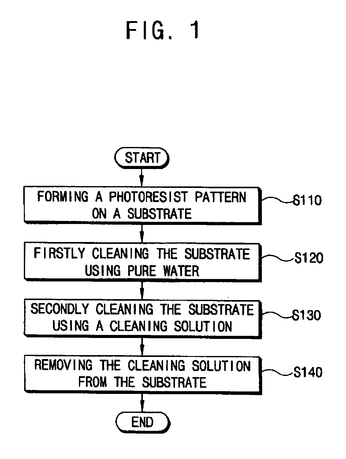
Cleaning solution and method of cleaning semiconductor devices using the same
a cleaning solution and semiconductor technology, applied in the direction of detergent compounding agents, instruments, photomechanical devices, etc., can solve the problems of easy generation of photoresist patterns, pattern becoming even more prone to deformation due to capillary force, and reducing the efficiency of cleaning solutions, so as to achieve high-integration semiconductor devices, reduce the risk of deformation, and prevent the effect of photoresist patterns
- Summary
- Abstract
- Description
- Claims
- Application Information
AI Technical Summary
Benefits of technology
Problems solved by technology
Method used
Image

Examples
example 1
Preparing Cleaning Solution
[0110] A cleaning solution was prepared by mixing 1.0 weight percent of octyl phenol ethoxylate (including about 10 mol of oxyethylene unit) and 99.0% by weight of pure water.
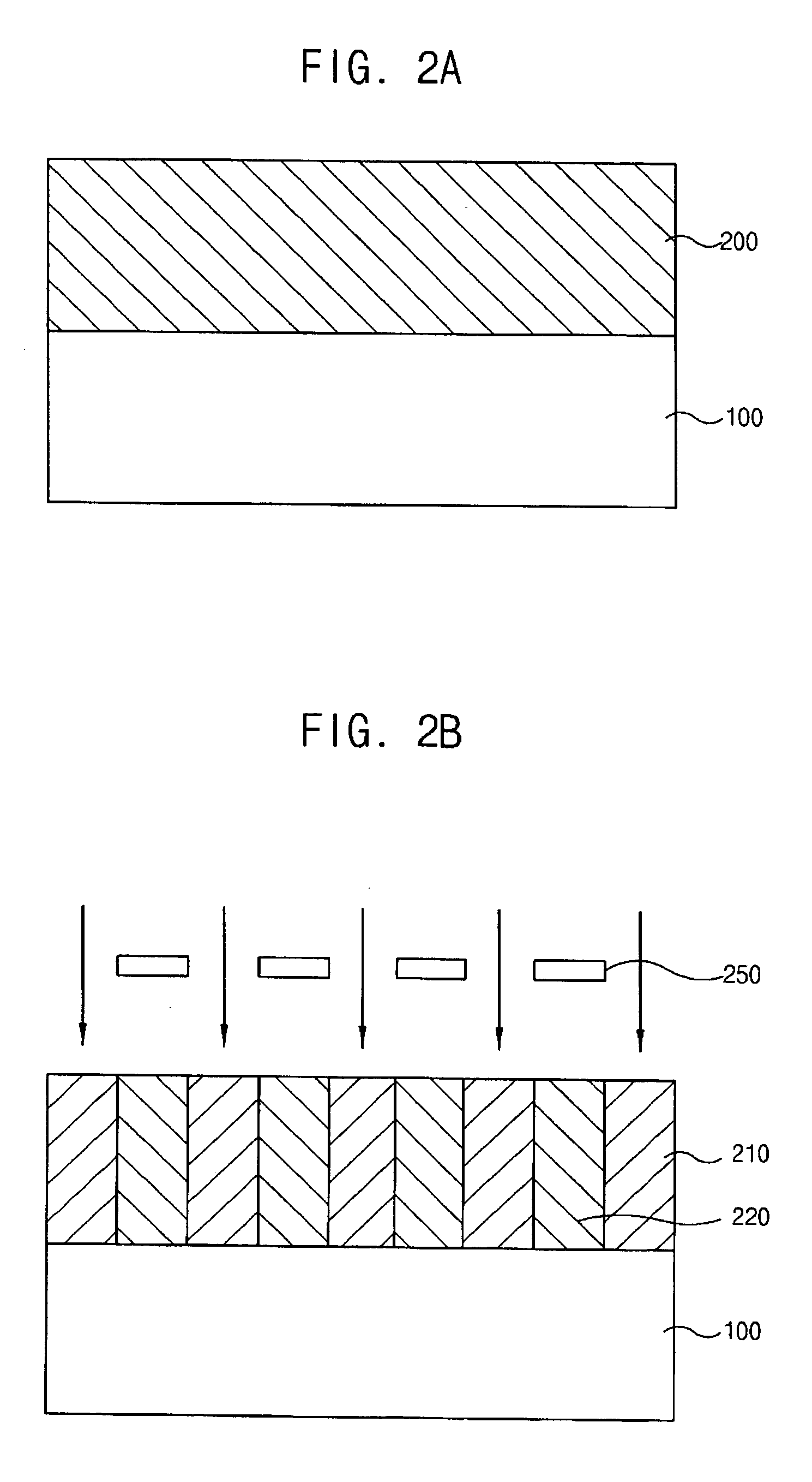
Forming Photoresist Patterns
[0111] A commercially available methacrylate photoresist (FARS-C20 manufactured by Fujifilm Arch Co., Ltd., Japan) for exposing to ArF was coated on a semiconductor wafer to have a thickness of about 2700 to about 2900 Å. Subsequently, the exposing amount for individual sectors on the wafer was adjusted using a mask including a test pattern having a pitch of 160 nm to adjust the width of patterns to be formed after developing. In particular, the pattern width was adjusted by 5 nm increments from 70 nm to 110 nm to obtain 9 different widths. The exposure process was carried out using a S306C ArF scanner (NA=0.78) manufactured by Nikon Co., Ltd. Then, the wafer was soft baked at about 110° C. for about 60 seconds and was developed using 2.38% TMAH aqueous...
examples 2-11
Preparing Cleaning Solutions
[0114] Cleaning solutions were prepared having different components from the solution prepared in Example 1. Detailed components are described in the following Table 1. The remaining component in the cleaning solution except the surfactant and the organic solvent was pure water.
[0115] As shown in Table 1, B represents octyl phenol ethoxylate (including about 10 mol of oxyethylene unit and about 2 mol of oxypropylene unit), C represents tetramethyl decyne diol, D represents decanol ethoxylate, E represents ammonium dioctyl sulfosuccinate, F represents Zonyl FSJ (fluoride-based surfactant commercially available from Du Pont Co., Ltd., U.S.A), and G represents L7614 (silicon-based surfactant commercially available from Union Carbide Co., Ltd., U.S.A). In Example 11, isopropyl alcohol was used as the organic solvent.
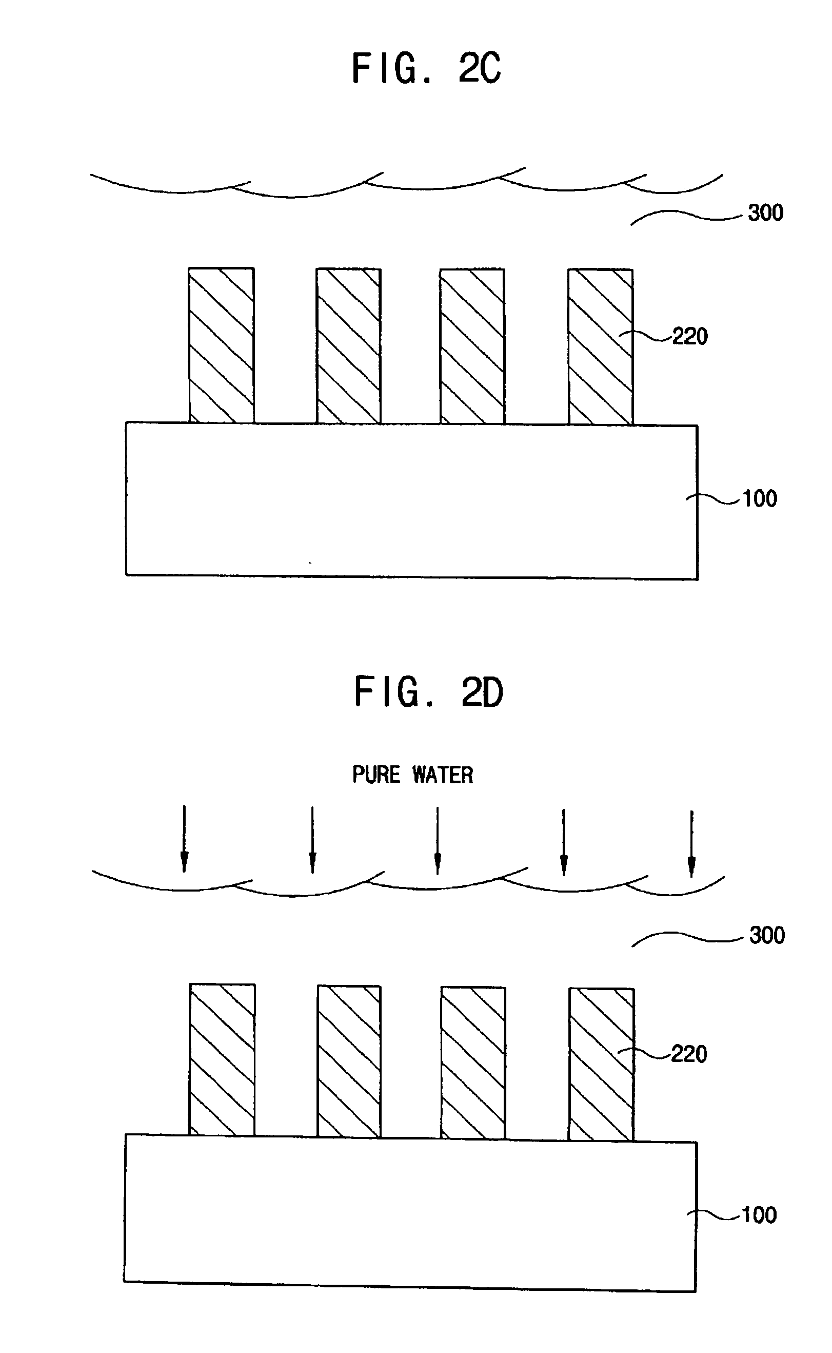
Cleaning
[0116] The same procedure from the forming of the photoresist patterns to the removing of the cleaning solution described in Exampl...
PUM
 Abstract
Description
Claims
Application Information