Pixel circuit

a pixel circuit and circuit technology, applied in the field of pixel circuits, can solve the problems of non-uniformity, non-uniformity, etc., and achieve the effects of reducing the time taken for initialisation and programming of the pixel circuit according to the present invention, reducing the time taken for pixel circuit initialisation and programming, and being more compact and compa

Inactive Publication Date: 2005-10-27
SEIKO EPSON CORP
View PDF0 Cites 47 Cited by
  • Summary
  • Abstract
  • Description
  • Claims
  • Application Information

AI Technical Summary

Benefits of technology

[0060] When in use, the time taken for initialisation and programming of the pixel circuit according to the present invention is reduced thereby providing a more efficient, faster and more versatile display system than in the prior art. The third signal em[n] used in the prior art is no longer required since the arrangement of the pixel circuit permits signals em[n] and scan[n] to be replaced by a single control signal. In a preferred embodiment, a reference signal supply line is no longer required thereby providing a more compact display system.
[0061] The number of control lines can also be reduced thereby also providing a more compact and efficient display system than is known from the prior art.

Problems solved by technology

Display systems employing an array of voltage driven pixel circuits as illustrated in FIG. 1 can experience non-uniformity problems in their displayed images even though individual driving TFTs in the array are supplied with an identical voltage data signal and supply voltage.
The non-uniformity arises due to a spatial variation in the threshold voltage of individual driving TFTs within the array of pixel circuits that form the display.

Method used


Image

  • Pixel circuit
  • Pixel circuit
  • Pixel circuit

Examples


first embodiment

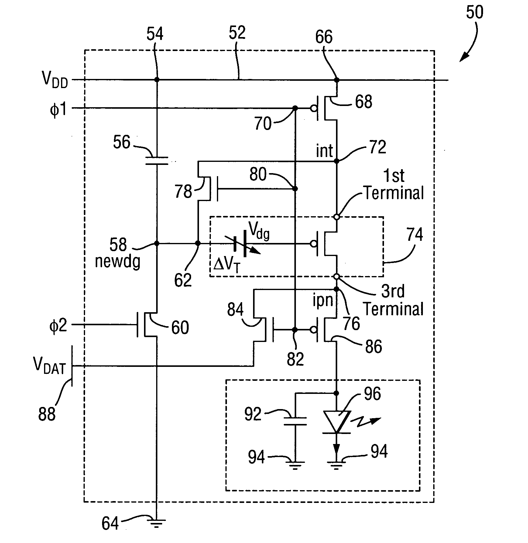
[0087] Referring to FIG. 4, a pixel circuit 50 according to the present invention comprises a first rail 52 having a first node 54 coupled to a first terminal of a first capacitor 56. A second terminal of the first capacitor 56 is coupled to a second node 58 (referred to as newdg) which is coupled to a source terminal of a first n-channel transistor 60 and a third node 62. The first n-channel transistor 60 comprises a gate terminal and also a drain terminal that is coupled to a second rail 64.

[0088] The first rail 52 comprises a fourth node 66 coupled to a source terminal of a first p-channel transistor 68 comprising a gate terminal coupled to a fifth node 70 and a drain terminal coupled to a sixth node 72 (referred to as int). The sixth node 72 int is coupled to a first terminal of the driver transistor 74 comprising a gate terminal and a third terminal. The driver transistor 74 is a second p-channel transistor. As best seen with reference to FIG. 3 and also described in detail lat...

second embodiment

[0107] Referring to FIG. 6, the pixel circuit 50 of FIG. 4 according to the present invention comprises an additional fourth p-channel transistor 98 comprising a source terminal coupled to the drain terminal of the third p-channel transistor 86 and a drain terminal coupled to the anode terminal of the OLED 96.

[0108] In operation, in the pre-charge stage, the second signal φ2 is applied to a gate terminal of the fourth p-channel transistor 98. The first n-channel transistor 60 is switched on and the fourth p-channel transistor 98 is switched off thereby isolating the OLED 96 during the pre-charge stage even if the first signal φ1 is logic 0 when the second signal φ2 is logic 1. The second embodiment therefore allows different driving waveforms to be used as described below with reference to FIGS. 11(a) and 11(b).

[0109] Referring to FIGS. 11(a) and (b), the second signal φ2 is logic 1 prior to the first signal φ1 becoming logic 1. If these driving waveforms were to be used in the cir...

third embodiment

[0110] Referring to FIG. 7, the pixel circuit 50 of FIG. 4 according to the present invention comprises an additional fifth p-channel transistor 102 and an additional fourth n-channel transistor 104. The fourth n-channel transistor 104 comprises a source terminal coupled to the first rail 52 and a drain terminal coupled to a node 108 referred to as newdg2. The node newdg2 is coupled to the third node 62—that is, node newdg2 and the third node 62 are technically the same—and to a first terminal of the fifth p-channel transistor 102. The fifth p-channel transistor 102 comprises a second terminal coupled to the second node 58 (newdg).

[0111] In operation, in the pre-charge stage, the second signal φ2 is applied to a gate terminal of the fourth n-channel transistor 104 and a gate terminal of the fifth p-channel transistor 102. When the second signal φ2 is logic 1 and the first n-channel transistor 60 is switched on, the fifth p-channel transistor 102 is switched off and the fourth n-chan...


PUM


Abstract

It is known to compensate for threshold voltage variation of driving transistors in pixel circuits that drive light emission devices such as current driven organic light emission devices. However, programming and initialisation of such pixel circuits can be slow and require a plurality of control or signal lines. The present invention provides a pixel circuit comprising an n-channel transistor for diode-connecting the driver transistor and a means for reducing the number of signal and control lines.

Description

BACKGROUND OF THE INVENTION [0001] 1. Field of the Invention [0002] The present invention relates, in general, to a pixel circuit of a type employed in a display system using a current driven organic or other light-emission device as a light source. [0003] 2. Description of the Prior Art [0004] Display systems commonly comprise an array of pixel circuits having an organic light-emitting device (OLED) as a light source and a driving circuit for driving the OLED in accordance with a received data signal. The OLED consists of a light-emitting polymer (LEP) layer sandwiched between an anode layer and a cathode layer. Electrically, the OLED operates as a diode whilst optically, the OLED emits light when forward biased with the brightness of the emitted light increasing as the forward bias current increases. By integrating the driving circuits of individual pixel circuits in the array using low-temperature polysilicon Thin Film Transistor (TFT) technology, it is possible to control the br...

Claims


Application Information

Patent Timeline
Patent Type & Authority Applications(United States)
IPC IPC(8): G09G3/20H01L51/50G09G3/30G09G3/32
CPCG09G3/3233G09G2300/0426G09G2300/0819G09G2320/043G09G2310/0262G09G2320/0233G09G2320/0252G09G2300/0842G09G3/30G09G3/20
Inventor TAM, SIMON
Owner SEIKO EPSON CORP
Why Eureka
Try Eureka