Integrated fet and schottky device

a technology of integrated fet and schottky, which is applied in the direction of instruments, transistors, acceleration measurement using interia forces, etc., can solve the problems of power application power loss, overall power loss of power circuit, power loss, etc., and achieve the effect of less power loss and more compactness

Inactive Publication Date: 2005-02-10
INFINEON TECH AMERICAS CORP
View PDF30 Cites 91 Cited by
  • Summary
  • Abstract
  • Description
  • Claims
  • Application Information

AI Technical Summary

Benefits of technology

[0004] To overcome the drawbacks of the prior art devices a device according to the present invention includes a schottky device and a power MOSFET both formed in a common die. As a result a device according to the present invention is more compact and exhibits less power loss.

Problems solved by technology

A major factor of concern in power applications is power loss.
Power loss in power applications may be in large part due to power losses by the power switching devices, such as power MOSFETs, within the power circuit.
For example, the power loss associated with the body diode of a power MOSFET is a factor that contributes to the overall power loss of a power circuit.
Such packages, however, are relatively large and exhibit undesirable transient behavior.

Method used


Image

  • Integrated fet and schottky device
  • Integrated fet and schottky device
  • Integrated fet and schottky device

Examples


first embodiment

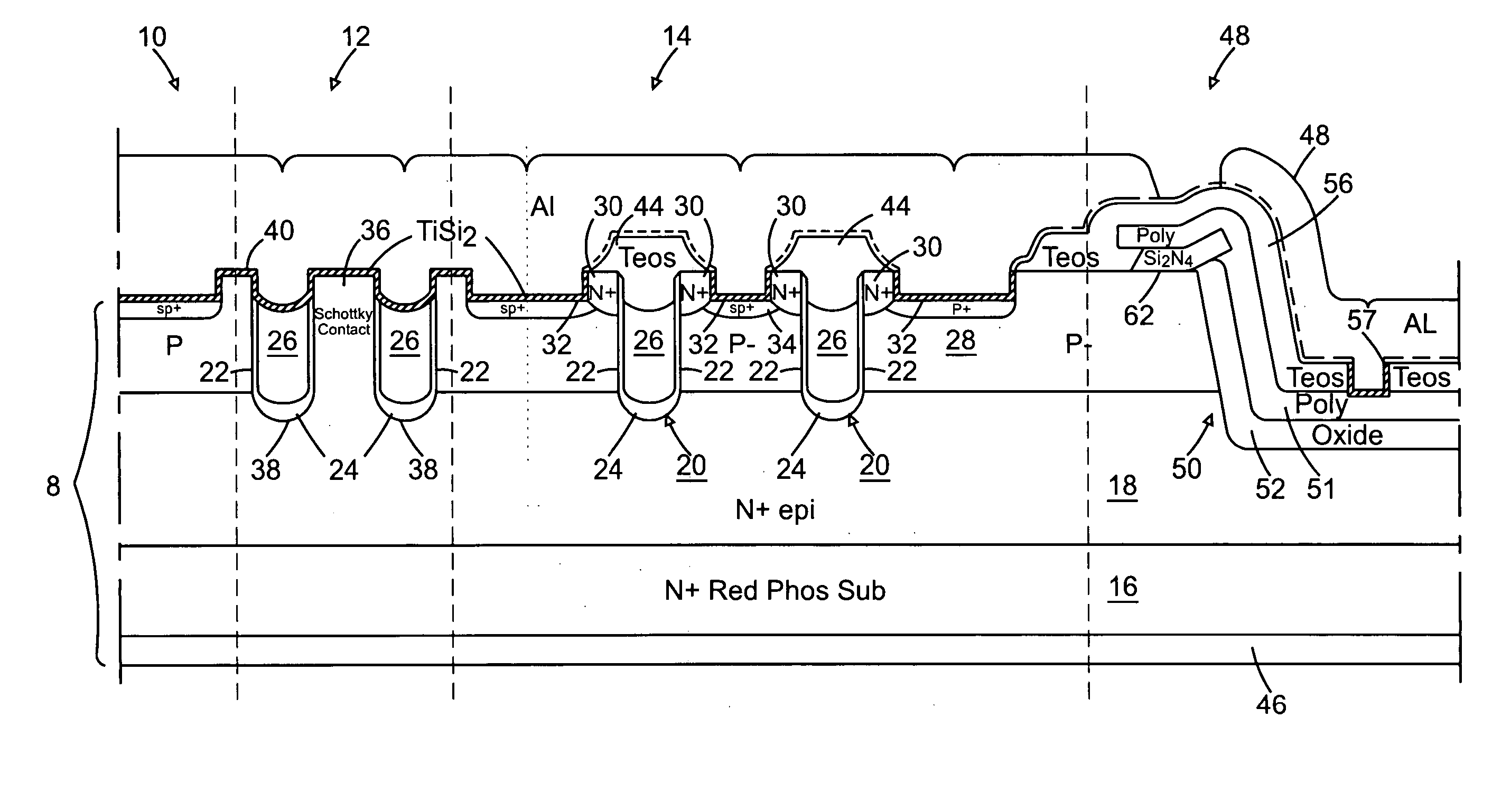
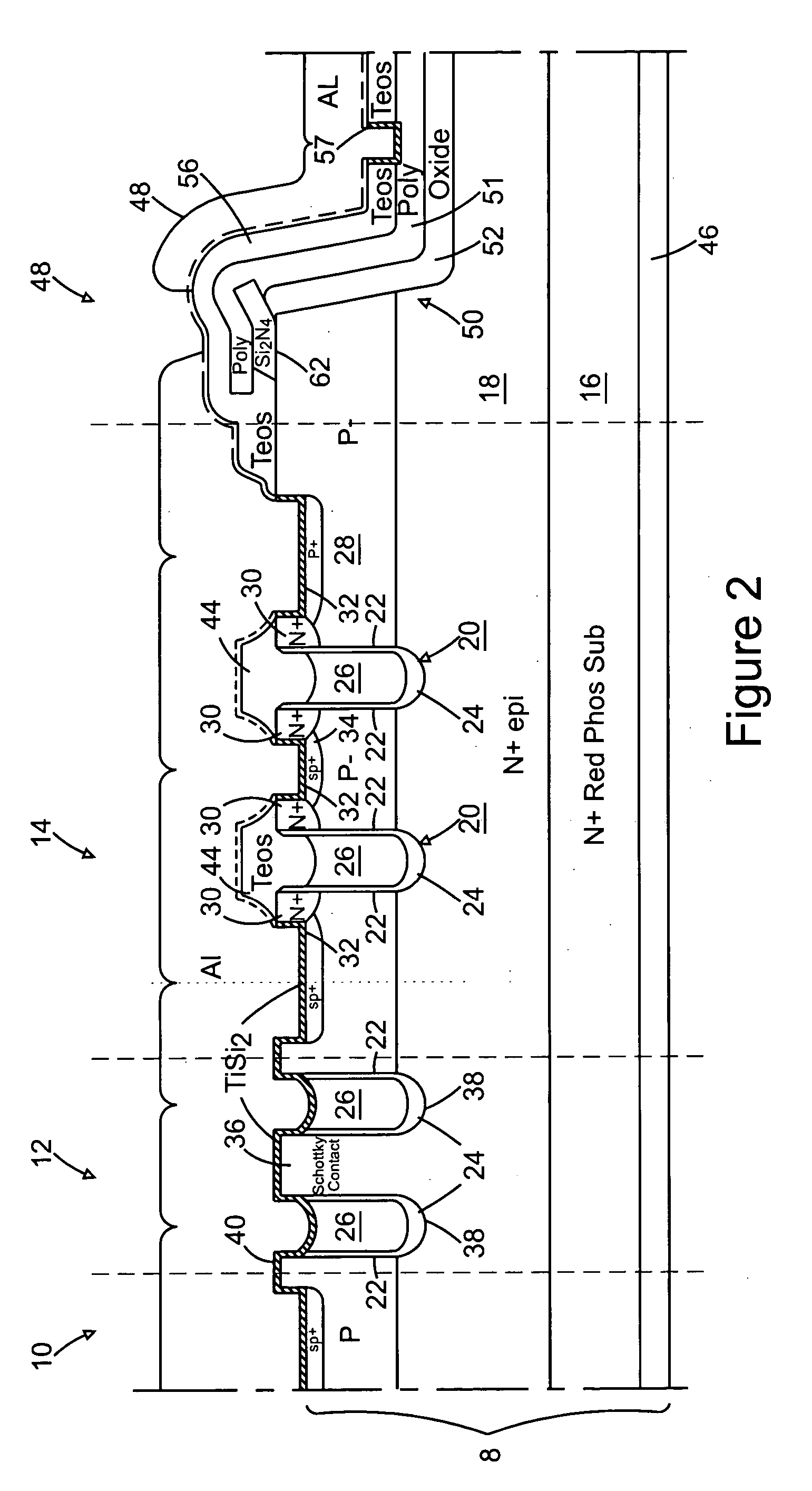
[0020] Referring to FIG. 2, a semiconductor device 10 according to the present invention includes at least one schottky region 12 and a field effect device that includes groups of gate structures 14 formed in a common die 8. Die 8 may include a highly doped substrate 16 of one conductivity type and a lightly doped epitaxial layer 18 of the one conductivity type formed over a major surface of substrate 16. Substrate 16 may be doped with red phosphorous although other highly-doped substrates may be used without deviating from the present invention.

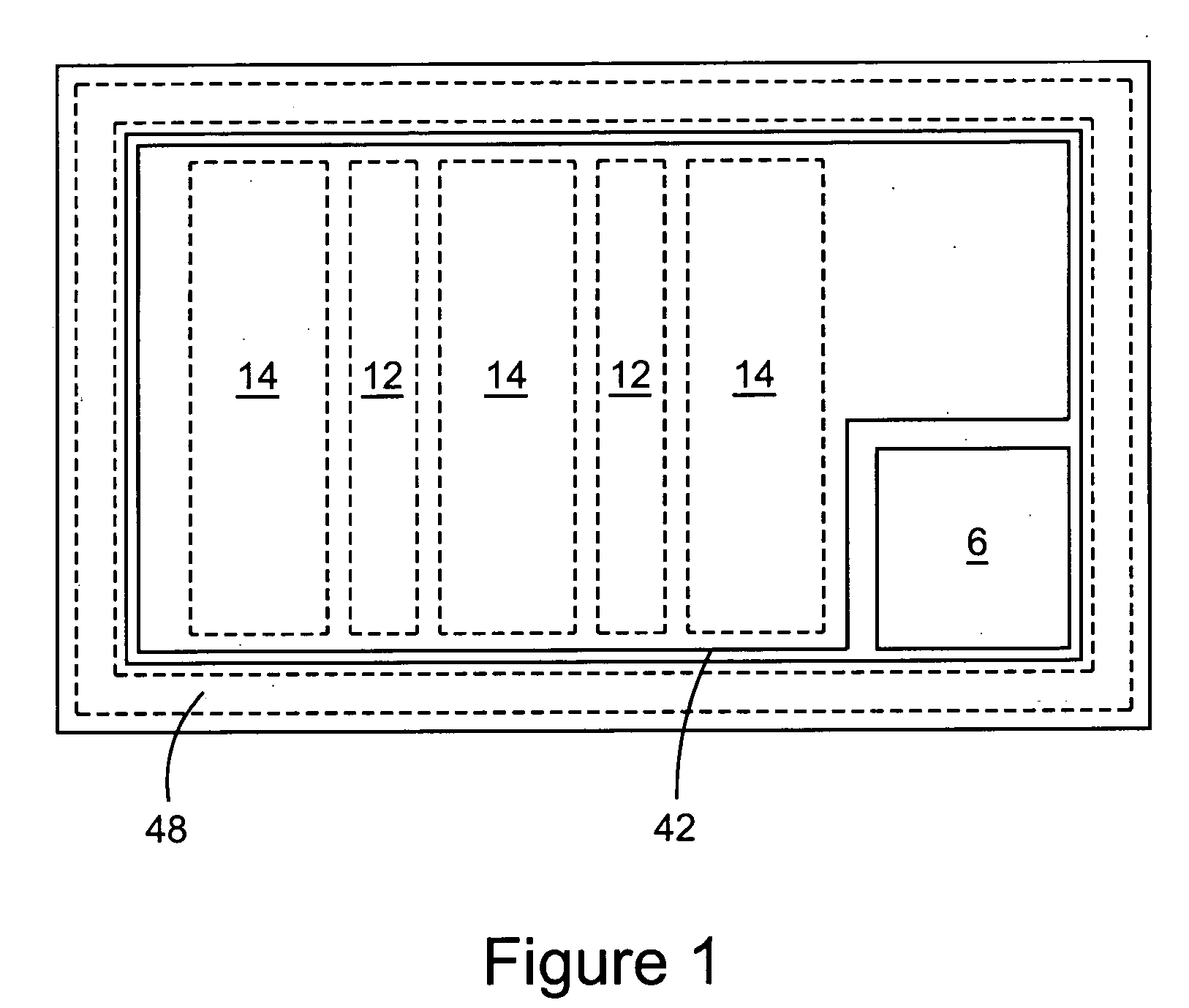
[0021] The field effect device in semiconductor device 10 according to the first embodiment of the present invention includes a plurality of gate structures similar to gate structures of known trench type devices. According to one aspect of the present invention each group of gate structures 14 is disposed adjacent a schottky region 12 as illustrated by FIG. 2.

[0022] Each trench 20 is formed in epitaxial layer 18 and includes gate oxide 22 ...

second embodiment

[0040] Referring to FIG. 8, device 78 according to the present invention is similar in all respects to device 10 except that the schottky region 12 of device 78 includes schottky barrier 80, which unlike schottky barrier 40 of device 10, only makes contact to the top surface of mesa 36 and does not extend to the sidewalls of trenches 38 and the polysilicon inside trenches 38.

[0041] The process for manufacturing device 78 according to the second embodiment has fewer mask steps than the process for manufacturing device 10 according to the first embodiment, and is carried out according to the process described above with reference to FIGS. 3-5 in combination with the following additional steps.

[0042] Referring next to FIG. 9, unlike the process set forth above for the manufacturing of device 10 (first embodiment) the layer of Si3N4 62 is not removed after the formation of conductive material 26 (i.e., deposition of polysilicon in trenches 20). Rather, without removing the layer of Si3...

third embodiment

[0047] Device 86 according to the present invention is manufactured according to the following process.

[0048] Referring first to FIG. 12, a layer of oxide is formed over the top surface of die 8. Next through photolithography and etch, portions of the layer of oxide are removed to open windows 89 in the layer of oxide to form layer of oxide 88 (solid line) and layer of oxide 92a (broken line), and expose part of the top surface of epitaxial layer 18 in window 89 area. Implanting through the window 89, counter-doped regions 92 are formed in epitaxial layer 18. Then a photoresist layer is formed over layer of oxide 88 and layer of oxide 92a is removed to expose part of the top surface of epitaxial layer 18. Using layer of oxide 88 (not removed by photolithography and etch) as a mask counter-doped regions 90 are formed in epitaxial layer 18. Thereafter, source dopants are implanted in the counter-doped regions 90 using layer of oxide 88 as a mask. It should be noted that source dopants...


PUM


Abstract

A semiconductor device including a schottky device and a trench type semiconductor switching device such as a MOSFET formed in a common die.

Description

FIELD OF THE INVENTION [0001] The present invention relates to a power semiconductor device and more particularly to a power semiconductor device which includes a schottky device and a MOSFET both formed in a common die. BACKGROUND OF THE INVENTION [0002] A major factor of concern in power applications is power loss. Power loss in power applications may be in large part due to power losses by the power switching devices, such as power MOSFETs, within the power circuit. For example, the power loss associated with the body diode of a power MOSFET is a factor that contributes to the overall power loss of a power circuit. [0003] The high frequency and high current demands of the modem power applications require the reduction of power loss. To prevent power loss from the body diode of a MOSFET it is known to use a schottky device in parallel with the body diode, which turns on at a lower voltage than the body diode to prevent conduction by the body diode of the MOSFET. Co-packaged MOSFET...

Claims


Application Information

Patent Timeline
Patent Type & Authority Applications(United States)
IPC IPC(8): H01L29/872H01L21/329H01L21/336H01L21/8234H01L21/8248H01L27/02H01L27/04H01L27/06H01L27/088H01L29/40H01L29/423H01L29/45H01L29/47H01L29/76H01L29/78
CPCH01L27/0629H01L29/407H01L29/42368H01L29/456H01L29/8725H01L29/7806H01L29/7811H01L29/7813H01L29/66727H01L2224/0603
Inventor HE, DONALDSODHI, RITUCHIOLA, DAVIDE
Owner INFINEON TECH AMERICAS CORP
Why Eureka
Try Eureka