Liquid crystal driving device, liquid crystal display device, analog buffer, and liquid crystal driving method

Inactive Publication Date: 2000-05-30
BOE TECH GRP CO LTD
View PDF13 Cites 87 Cited by
  • Summary
  • Abstract
  • Description
  • Claims
  • Application Information

AI Technical Summary

Problems solved by technology

Conversely, however, it suffers from the drawbacks of susceptibility to horizontal cross-talk and visible horizontal stripes in video displays.
Large liquid crystal panels, however, suffer from a brightness gradient problem caused by parasitic resistance of the interconnect electrodes.
The brightness gradient problem cannot be solved by means of 1H inversion driving.
Conversely, however, it suffers from the drawbacks of susceptibility to vertical cross-talk and visible vertical stripes in video displays.
Although it is possible solve the brightness gradient problem mentioned above, using elements which have large off leakage currents leads to undesirable effects.
Further, the realization of this method means that the configuration and control of the driver circuits become extremely complex, thus creating the disadvantages of longer design times and higher device costs.
However, these design conditions are sometimes changed in the development process; and a change in any of the said design conditions after one of the said four methods has already been adopted will also necessitate a change in the driving method, a matter that requires tremendous labor for circuit changes a

Method used


Image

  • Liquid crystal driving device, liquid crystal display device, analog buffer, and liquid crystal driving method
  • Liquid crystal driving device, liquid crystal display device, analog buffer, and liquid crystal driving method
  • Liquid crystal driving device, liquid crystal display device, analog buffer, and liquid crystal driving method

Examples


first embodiment

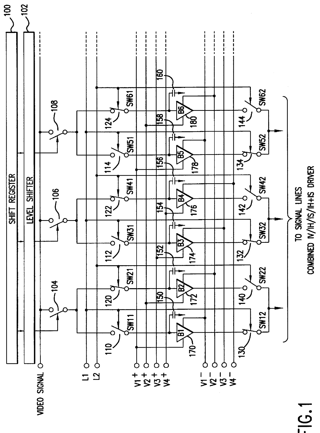
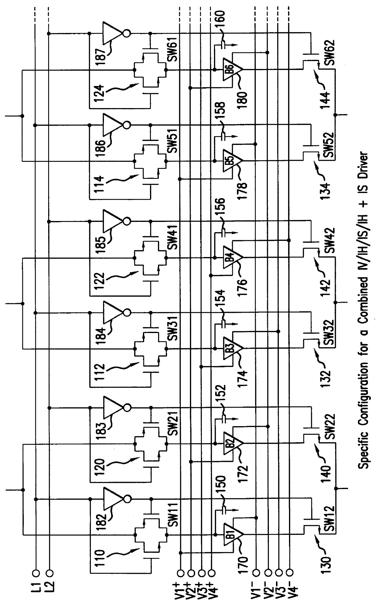
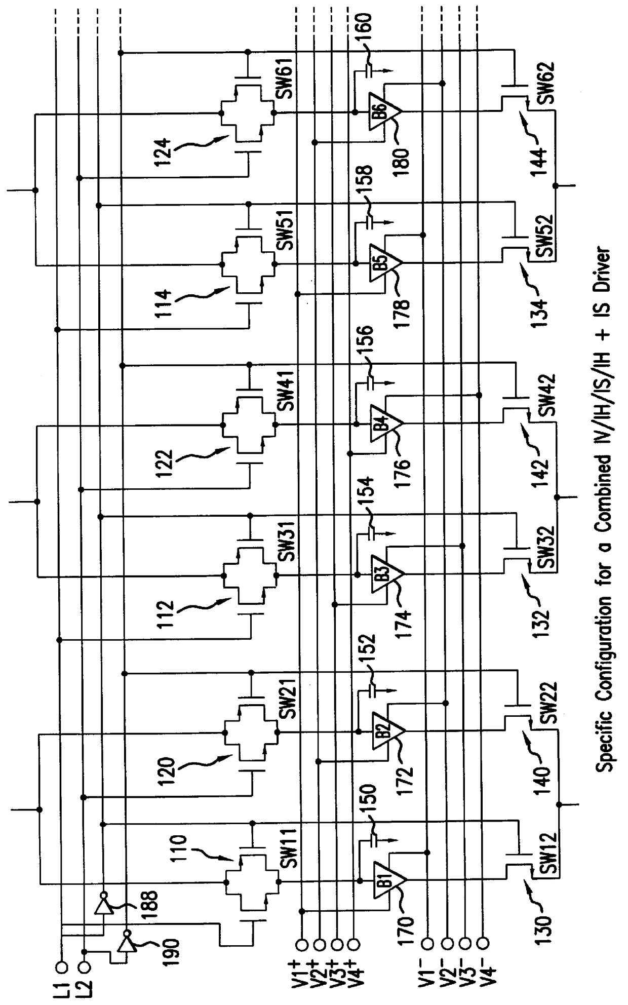
FIG. 1 shows an example of the configuration of a liquid crystal driver (liquid crystal driving device) according to the first embodiment of this invention. The first embodiment concerns a combined 1V / 1H / 1S / 1H+1S liquid crystal driver. This liquid crystal driver is known as a source driver which drives the signal lines and includes multiple (1 to N) signal driving means. For example, the first signal driving means includes switches (analog switches) 104, 110, 120, 130, 140; capacitors 150 and 152; and analog buffers 170 and 172. The second signal driving means includes switches 106, 112, 122, 132, 142; capacitors 154 and 156; and analog buffers 174 and 176. Additionally, the number of signal lines in FIG. 1 driven by the liquid crystal driver is, for the display of color on a 640.times.480 dot liquid crystal panel, for example, 640.times.3. In this case, it is acceptable to provide multiple liquid crystal driver devices to drive these signal lines, or it is also acceptable to locate...

second embodiment

The configuration of a second embodiment of this invention is shown in FIG. 14. The second embodiment relates to a liquid crystal driver for dedicated 1V driving. In this embodiment and those which follow, the shift register, level shifter, and sampling switches are omitted from the explanations. As in the first embodiment, there are two switch control lines in the second embodiment. Switching control is achieved through switch control line L1 for the first and third switches including 110, 130, 112, 132, 114, and 134 while switching control is achieved through switch control line L2 for the second and fourth switches including 120, 140, 122, 142, 124, and 144. Although there was a four-channel supply in the first embodiment, in this second embodiment there are only V.sup.+ and V.sup.- supply lines forming a single channel system. In other words, all analog buffers 170 to 180 are connected to common supply lines; and the supply voltages applied to the common supply lines are control...

third embodiment

The configuration of a third embodiment of this invention is shown in FIG. 16. The third embodiment relates to a liquid crystal driver for dedicated 1H driving. As in the first embodiment, there are two switch control lines in the third embodiment. Although there was a four-channel supply in the first embodiment, in this third embodiment there are Vodd.sup.+, Vodd.sup.-, Veven.sup.+, and Veven.sup.- supply lines forming a two-channel system. The first analog buffers 170, 174, and 178 receive supply voltages from the first supply lines Vodd.sup.+ and Vodd.sup.-whereas the second analog buffers 172, 176, and 180 receive supply voltages from the second supply lines Veven.sup.+ and Veven.sup.-. As a result, analog buffers 170, 174 and 178 can be made to differ in polarity from analog buffers 172, 176, and 180.

FIG. 17 shows the timing chart for achieving 1H inversion driving with the liquid crystal driver of FIG. 16. The third embodiment operates similarly to the operations explained in ...


PUM


Abstract

PCT No. PCT/JP95/02369 Sec. 371 Date Oct. 28, 1996 Sec. 102(e) Date Oct. 28, 1996 PCT Filed Nov. 21, 1995 PCT Pub. No. WO96/16347 PCT Pub. Date May 30, 1996A video signal is sampled by sequential switches (104), etc. and the voltage held in capacitors (150) after passing through switches (110). Next, switches (120), (130) turn on, the hold for capacitor (152) is carried out, and that voltage buffered by analog buffer (170), then output. The switch on-off control is performed by means of lines L1 and L2. The control of the supply voltage is performed by V1+ to V4+, and the polarity of analog buffers (170), (172), etc. is controlled. By means of the switch on-off control and the supply voltage control, four driving methods for alternating liquid crystal driving can be realized. Further, the analog buffers are composed of TFTs; and positive and negative polarity inversion can be performed through supply voltage shift.

Description

FIELD OF TECHNOLOGYThis invention pertains to a driving method for a liquid crystal panel and, in particular, a driving method for a TFT liquid crystal panel.BACKGROUND TECHNOLOGYA number of different driving methods for TFT liquid crystal panels are already known. For example, as stated in "Driver LSI Problems Solved by low Voltage Single Power Supply", Flat Panel Display 1991 (Nov. 26, 1990, Nikkei Business Publications, Inc., p. 168 to p. 172), TFT liquid crystal panel drivers (liquid crystal driving devices) can be broadly divided into two types: digital and analog. The typical structure of a conventional analog line sequential driver is shown in FIG. 38. This conventional driver contains shift register 2000, level shifter 2002, switches (analog switches) 2004 to 2018, sampling capacitors 2020 to 2026, hold capacitors 2028 to 2034, and analog buffers 2036 to 2042. Shift register 2000 shifts in synchronization with the shift clock, the output is input into level shifter 2002, and...

Claims


Application Information

Patent Timeline
IPC IPC(8): G09G3/36G09G3/20
CPCG09G3/3614G09G3/3688G09G3/2011G09G3/3659G09G2330/021G09G2310/0297G09G2320/0209G09G2320/0247G09G2310/0291G02F1/133G09G3/36
Inventor OZAWA, TOKUROH
Owner BOE TECH GRP CO LTD
Why Eureka
Try Eureka