Silicon based solid state lighting

a solid-state lighting and silicon-based technology, applied in the direction of semiconductor/solid-state device manufacturing, semiconductor structures, electrical equipment, etc., can solve the problems of low manufacturing throughput of conventional solid-state lighting devices. , to achieve the effect of preventing cracking or delamination, preventing associated layer cracking, and increasing light emission efficiency

Inactive Publication Date: 2011-05-12
SIPHOTON
View PDF53 Cites 83 Cited by
  • Summary
  • Abstract
  • Description
  • Claims
  • Application Information

AI Technical Summary

Benefits of technology

[0011]An advantage associated with the disclosed LED structures and fabrication processes can overcome latter mismatch between the group III-V layer and the substrate and prevent associated layer cracking in conventional LED structures. The disclosed LED structures and fabrication processes can also prevent cracking or delamination in the p-doped or n-doped group III-V nitride layer caused by different thermal expansions between the p-doped group III-V nitride layer and the substrate. An advantage associated with the disclosed LED structures is that LED structures can significantly increase light emission efficiency by increasing densities of the LED structures and by additional light emissions from the sloped or vertical surfaces in the trenches.
[0012]Another advantage associated with the disclosed LED structures and fabrication processes is that the disclosed LED structures can be fabricated using existing commercial semiconductor processing equipment such as ALD and MOCVD systems. The disclosed LED fabrication processes can thus be more efficient in cost and time that some conventional LED structures that need customized fabrication equipments. The disclosed LED fabrication processes are also more suitable for high-volume semiconductor lighting device manufacture. Silicon wafers or glass substrates can be used to produce solid state LEDs. Manufacturing throughput can be much improved since silicon wafer can be provided in much larger dimensions (e.g. 6 to 12 inch silicon wafers) compared to the substrates used in the conventional LED structures. Furthermore, the silicon-based substrate can also allow driving and control circuit to be fabricated in the substrate. The LED device can thus be made more integrated and compact than conventional LED devices.
[0013]Yet another advantage of the disclosed LED structures and fabrication processes is that a transparent conductive layer can be formed on the upper III-V nitride layer of the LED structures to increase electric contact between the upper electrode and the upper Group III-V layer, and at the same time, maximizing light emission intensity from the upper surfaces of the LED structures.
[0014]Embodiments may include one or more of the following advantages. The disclosed lighting device and related fabrication processes can provide light devices at higher manufacturing throughput and thus manufacturing cost compared to the conventional light devices. The disclosed lighting device and related fabrication processes can also provide more integrated light devices that can include light emitting element, a driver, power supply, and light modulation unit integrated on a single semiconductor substrate.

Problems solved by technology

Although solid-state lighting offers certain advantages, conventional semiconductor structures and devices used for solid-state lighting are relatively expensive.
One of the costs related to conventional solid-state lighting devices is related to the relatively low manufacturing throughput of the conventional solid-state lighting devices.
One drawback of the above described convention LED structure 100 is the low manufacturing throughput associated with the small substrate dimensions.
Another drawback of the above described convention LED structure 100 is that the suitable substrates such as sapphire or silicon carbide are typically not provided in single crystalline forms.
As a result, light emitting performance of the LED structure 100 can be compromised.

Method used


Image

  • Silicon based solid state lighting
  • Silicon based solid state lighting
  • Silicon based solid state lighting

Examples


Embodiment Construction

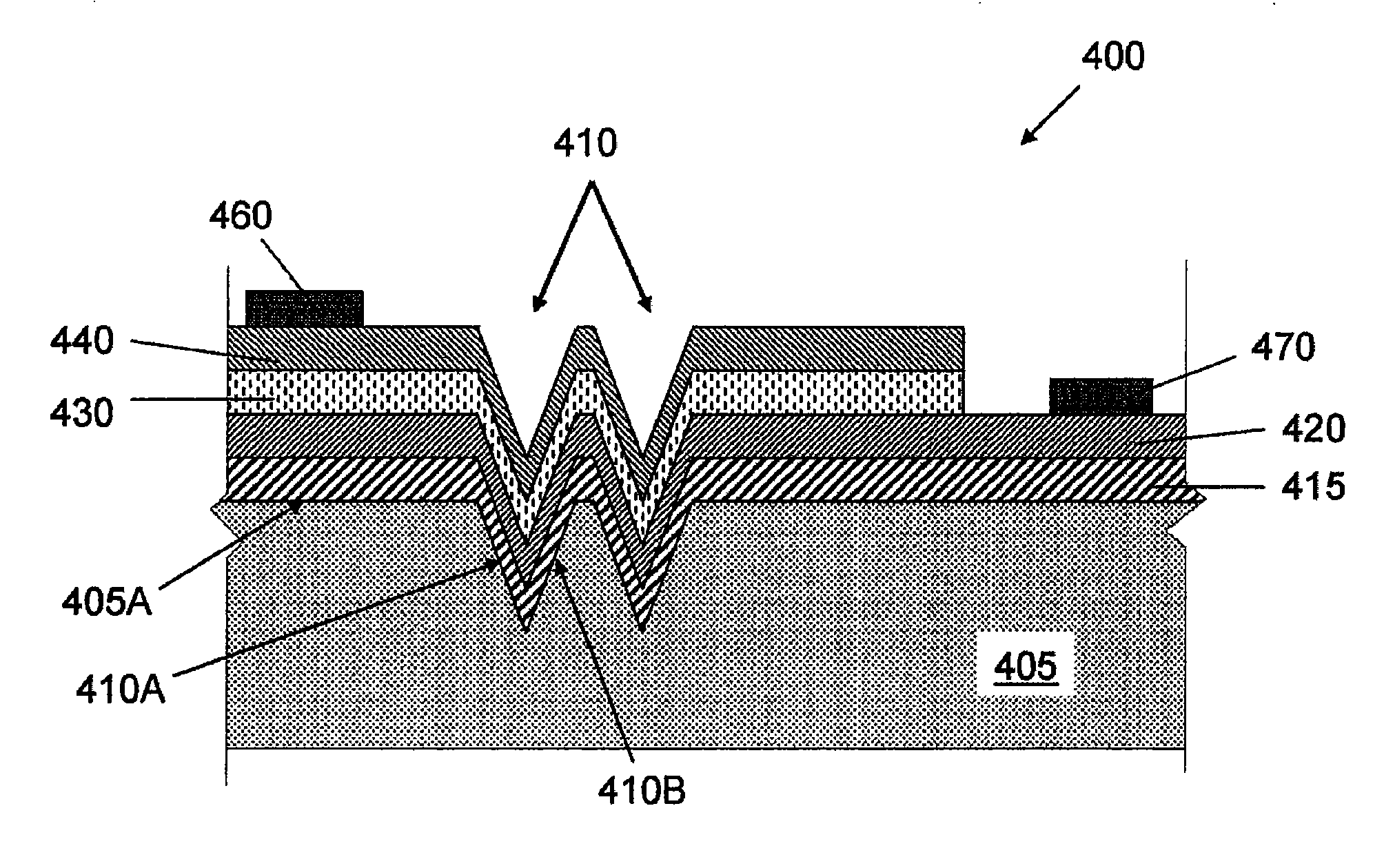
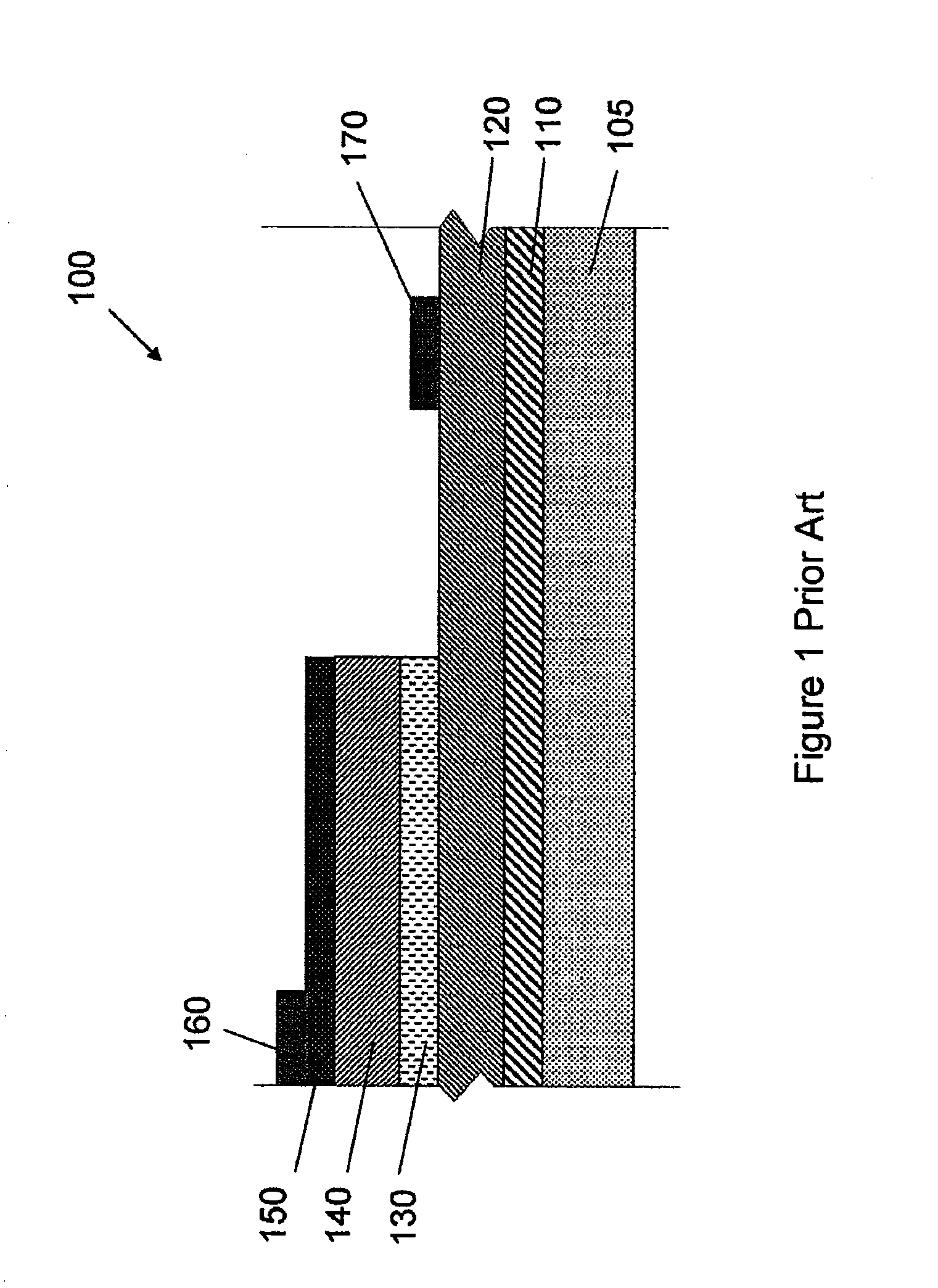
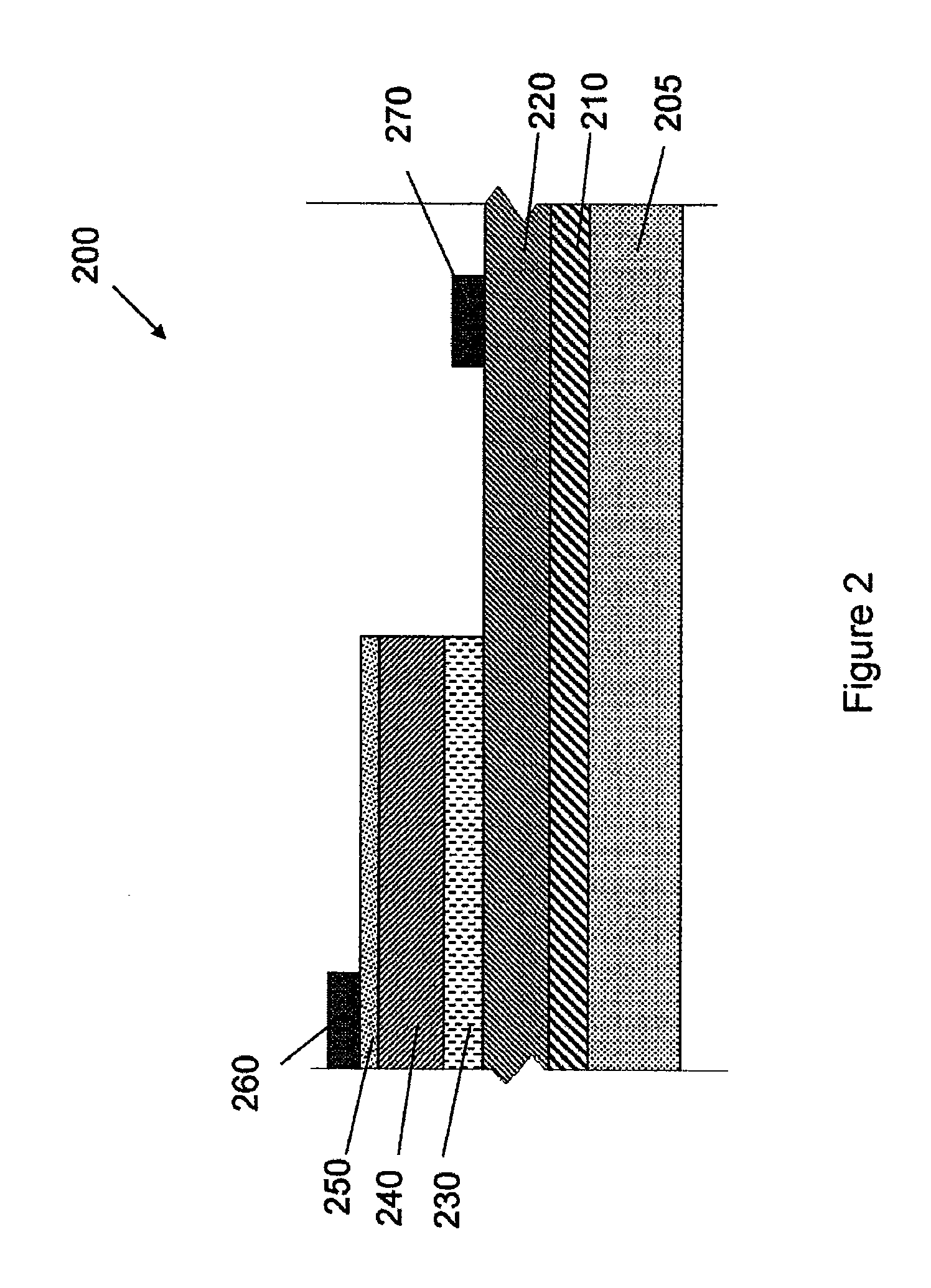
[0026]Referring to FIG. 2, a LED structure 200 includes a substrate 205, which can have an upper surface in the (111) or a (100) crystalline direction. The substrate 205 can be formed by silicon, silicon oxide, or glass. For a silicon substrate, the substrate 205 can include a (100) or (111) upper surface. The substrate 205 can also include a complimentary metal oxide semiconductor (CMOS) material that includes an electric circuitry for driving and controlling the LED structure 200. A buffer layer 210 is formed on the substrate 205. The buffer layer 210 can be formed of GaN, ZnO, MN, HfN, AlAs, TaN, or SiC. As described below in more details in conjunction with FIG. 6, the buffer layer 210 is deposited on the substrate 205 using atomic layer deposition (ALD) in a vacuum chamber maintained at a temperature in the range of 450° C. to 750° C., such as about 600° C. The buffer layer 210 can have a thickness of about 1 to 1000 Angstroms such as 10 to 100 Angstroms. The buffer layer 210 c...


PUM

PropertyMeasurementUnit
thicknessaaaaaaaaaa
temperatureaaaaaaaaaa

Abstract

A semiconductor device includes a substrate comprising a first surface having a first orientation and a second surface having a second orientation and a plurality of III-V nitride layers on the substrate, wherein the plurality of III-V nitride layers are configured to emit light when an electric current is produced in one or more of the plurality of III-V nitride layers.

Description

BACKGROUND[0001]The present patent application is related to solid-state lighting devices.[0002]Solid-state light sources, such as light emitting diodes (LEDs) and laser diodes, can offer significant advantages over other forms of lighting, such as incandescent or fluorescent lighting. For example, when LEDs or laser diodes are placed in arrays of red, green and blue elements, they can act as a source for white light or as a multi-colored display. In such configurations, solid-state light sources are generally more efficient and produce less heat than traditional incandescent or fluorescent lights. Although solid-state lighting offers certain advantages, conventional semiconductor structures and devices used for solid-state lighting are relatively expensive. One of the costs related to conventional solid-state lighting devices is related to the relatively low manufacturing throughput of the conventional solid-state lighting devices.[0003]Referring to FIG. 1, a conventional LED struc...

Claims


Application Information

Patent Timeline
Patent Type & Authority Applications(United States)
IPC IPC(8): H01L29/66H01L33/04H01L33/00H01L33/12H01L33/16
CPCH01L21/0237H01L21/02381H01L21/0243H01L21/02433H01L33/16H01L21/02502H01L21/0254H01L33/007H01L33/12H01L21/02439
Inventor PAN, SHAOHER X.
Owner SIPHOTON
Why Eureka
Try Eureka